SNVS541H October 2007 – August 2016 LM3410 , LM3410-Q1
PRODUCTION DATA.
- 1 Features
- 2 Applications
- 3 Description
- 4 Revision History
- 5 Pin Configuration and Functions
- 6 Specifications
- 7 Detailed Description
-
8 Application and Implementation
- 8.1 Application Information
- 8.2
Typical Applications
- 8.2.1 Low Input Voltage, 1.6-MHz, 3 to 5 White LED Output at 50-mA Boost Converter
- 8.2.2 LM3410X SOT-23: 5 × 1206 Series LED String Application
- 8.2.3 LM3410Y SOT-23: 5 × 1206 Series LED String Application
- 8.2.4 LM3410X WSON: 7 × 5 LED Strings Backlighting Application
- 8.2.5 LM3410X WSON: 3 × HB LED String Application
- 8.2.6 LM3410Y SOT-23: 5 × 1206 Series LED String Application With OVP
- 8.2.7 LM3410X SEPIC WSON: HB or OLED Illumination Application
- 8.2.8 LM3410X WSON: Boost Flash Application
- 8.2.9 LM3410X SOT-23: 5 × 1206 Series LED String Application With VIN > 5.5 V
- 8.2.10 LM3410X WSON: Camera Flash or Strobe Circuit Application
- 8.2.11 LM3410X SOT-23: 5 × 1206 Series LED String Application With VIN and VPWR Rail > 5.5 V
- 8.2.12 LM3410X WSON: Boot-Strap Circuit to Extend Battery Life
- 9 Power Supply Recommendations
- 10Layout
- 11Device and Documentation Support
- 12Mechanical, Packaging, and Orderable Information
封装选项
机械数据 (封装 | 引脚)
散热焊盘机械数据 (封装 | 引脚)
- DGN|8
订购信息
10 Layout
10.1 Layout Guidelines
When planning layout there are a few things to consider when trying to achieve a clean, regulated output. The most important consideration when completing a boost converter layout is the close coupling of the GND connections of the COUT capacitor and the PGND pin. The GND ends must be close to one another and be connected to the GND plane with at least two vias. There must be a continuous ground plane on the bottom layer of a two-layer board except under the switching node island. The FB pin is a high impedance node and the FB trace must be kept short to avoid noise pickup and inaccurate regulation. The RSET feedback resistor must be placed as close as possible to the IC, with the AGND of RSET (R1) placed as close as possible to the AGND of the IC. Radiated noise can be decreased by choosing a shielded inductor. The remaining components must also be placed as close as possible to the IC. See AN-1229 SIMPLE SWITCHER® PCB Layout Guidelins (SNVA054) for further considerations and the LM3410 demo board as an example of a four-layer layout.
For certain high power applications, the PCB land may be modified to a dog bone shape (see Figure 33). Increasing the size of ground plane and adding thermal vias can reduce the RθJA for the application.
10.2 Layout Examples
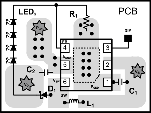 Figure 32. Boost PCB Layout Guidelines
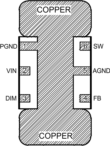 Figure 33. PCB Dog Bone Layout
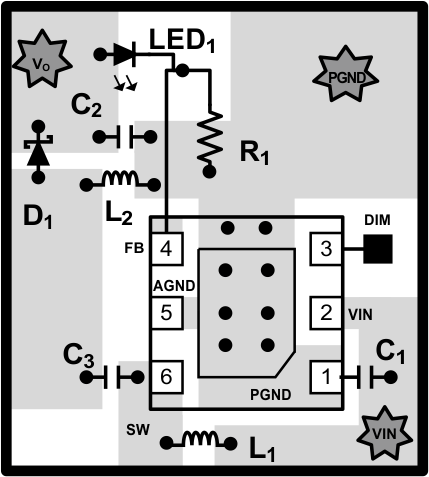
10.3 Thermal Considerations
10.3.1 Design
When designing for thermal performance, many variables must be considered, such as ambient temperature, airflow, external components, and PCB design.
The surrounding maximum air temperature is fairly explanatory. As the temperature increases, the junction temperature increases. This may not be linear though. As the surrounding air temperature increases, resistances of semiconductors, wires and traces increase. This decreases the efficiency of the application, and more power is converted into heat, and increases the silicon junction temperatures further.
Forced air can drastically reduce the device junction temperature. Air flow reduces the hot spots within a design. Warm airflow is often much better than a lower ambient temperature with no airflow.
Choose components that are efficient, and the mutual heating between devices can be reduced.
The PCB design is a very important step in the thermal design procedure. The LM3410 and LM3410-Q1 are available in three package options (6-pin WSON, 8-pin MSOP, and 5-pin SOT-23). The options are electrically the same, but there are differences between the package sizes and thermal performances. The WSON and MSOP have thermal die attach pads (DAP) attached to the bottom of the packages, and are therefore capable of dissipating more heat than the SOT-23 package. It is important that the customer choose the correct package for the application. A detailed thermal design procedure has been included in this data sheet. This procedure helps determine which package is correct, and common applications are analyzed.
There is one significant thermal PCB layout design consideration that contradicts a proper electrical PCB layout design consideration. This contradiction is the placement of external components that dissipate heat. The greatest external heat contributor is the external Schottky diode. Increasing the distance between the LM3410 or LM3410-Q1 and the Schottky diode may reduce the mutual heating effect. This, however, creates electrical performance issues. It is important to keep the device, the output capacitor, and Schottky diode physically close to each other (see Layout Guidelines). The electrical design considerations outweigh the thermal considerations. Other factors that influence thermal performance are thermal vias, copper weight, and number of board layers.
Heat energy is transferred from regions of high temperature to regions of low temperature via three basic mechanisms: radiation, conduction and convection. Conduction and convection are the dominant heat transfer mechanism in most applications.
The data sheet values for each packages thermal impedances are given to allow comparison of the thermal performance of one package against another. To achieve a comparison between packages, all other variables must be held constant in the comparison (PCB size, copper weight, thermal vias, power dissipation, VIN, VOUT, load current, and others). This provides indication of package performance, but it would be a mistake to use these values to calculate the actual junction temperature in an application.
10.3.2 LM3410 and LM3410-Q1 Thermal Models
Heat is dissipated from the LM3410, LM3410-Q1, and other devices. The external loss elements include the Schottky diode, inductor, and loads. All loss elements mutually increase the heat on the PCB, and therefore increase each other’s temperatures.
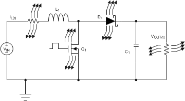 Figure 35. Thermal Schematic
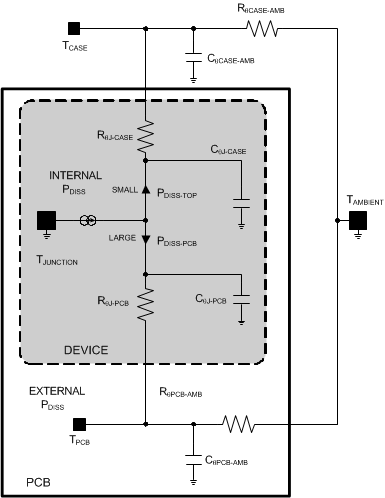 Figure 36. Associated Thermal Model
10.3.3 Calculating Efficiency and Junction Temperature
Use Equation 31 to calculate RθJA.

A common error when calculating RθJA is to assume that the package is the only variable to consider.
Other variables are:
- Input voltage, output voltage, output current, RDS(ON)
- Ambient temperature and air flow
- Internal and external components' power dissipation
- Package thermal limitations
- PCB variables (copper weight, thermal vias, and component placement)
Another common error when calculating junction temperature is to assume that the top case temperature is the proper temperature when calculating RθJC. RθJC represents the thermal impedance of all six sides of a package, not just the top side. This document refers to a thermal impedance called RΨJC. RΨJC represents a thermal impedance associated with just the top case temperature. This allows for the calculation of the junction temperature with a thermal sensor connected to the top case.
The complete LM3410 and LM3410-Q1 boost converter efficiency can be calculated using Equation 32.
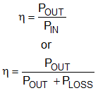
where
- PLOSS is the sum of two types of losses in the converter, switching and conduction
Conduction losses usually dominate at higher output loads, where as switching losses remain relatively fixed and dominate at lower output loads.
To calculate losses in the LM3410 or LM3410-Q1 device, use Equation 33.
where
- PQ = quiescent operating power loss
Conversion ratio of the boost converter with conduction loss elements inserted is calculated with Equation 34.

where
- RDCR is the Inductor series resistance

If the loss elements are reduced to zero, the conversion ratio simplifies to Equation 36.


Therefore:
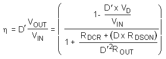
Only calculations for determining the most significant power losses are discussed. Other losses totaling less than 2% are not discussed.
A simple efficiency calculation that takes into account the conduction losses is Equation 39.
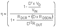
The diode, NMOS switch, and inductor (DCR) losses are included in this calculation. Setting any loss element to zero simplifies the equation.
VD is the forward voltage drop across the Schottky diode. It can be obtained from Electrical Characteristics.
Conduction losses in the diode are calculated with Equation 40.
Depending on the duty cycle, this can be the single most significant power loss in the circuit. Choose a diode that has a low forward voltage drop. Another concern with diode selection is reverse leakage current. Depending on the ambient temperature and the reverse voltage across the diode, the current being drawn from the output to the NMOS switch during time (D) could be significant, this may increase losses internal to the LM3410 or LM3410-Q1 and reduce the overall efficiency of the application. See the Schottky diode manufacturer’s data sheets for reverse leakage specifications.
Another significant external power loss is the conduction loss in the input inductor. The power loss within the inductor can be simplified to Equation 41,
Or Equation 42.

The LM3410 and LM3410-Q1 conduction loss is mainly associated with the internal power switch.
 Figure 37. LM3410 and LM3410-Q1 Switch Current

(small ripple approximation)
Or

The value for RDS(ON) must be equal to the resistance at the desired junction temperature for analyzation. As an example, at 125°C and RDS(ON) = 250 mΩ (See Typical Characteristics for value).
Switching losses are also associated with the internal power switch. They occur during the switch ON and OFF transition periods, where voltages and currents overlap resulting in power loss.
The simplest means to determine this loss is empirically measuring the rise and fall times (10% to 90%) of the switch at the switch node.
Table 25. Typical Switch-Node Rise and Fall Times
| VIN (V) | VOUT (V) | tRISE (ns) | tFALL (ns) |
|---|---|---|---|
| 3 | 5 | 6 | 4 |
| 5 | 12 | 6 | 5 |
| 3 | 12 | 8 | 7 |
| 5 | 18 | 10 | 8 |
10.3.3.1 Quiescent Power Losses
IQ is the quiescent operating current, and is typically around 1.5 mA.
10.3.4 Example Efficiency Calculation
Operating Conditions:5 × 3.3-V LEDs + 190 mVREF ≊ 16.7 V
Table 26. Operating Conditions
| PARAMETER | VALUE |
|---|---|
| VIN | 3.3 V |
| VOUT | 16.7 V |
| ILED | 50 mA |
| VD | 0.45 V |
| fSW | 1.6 MHz |
| IQ | 3 mA |
| tRISE | 10 ns |
| tFALL | 10 ns |
| RDS(ON) | 225 mΩ |
| LDCR | 75 mΩ |
| D | 0.82 |
| IIN | 0.31 A |
Quiescent Power Loss:
Switching Power Loss:
Internal NFET Power Loss:
Diode Loss:
Inductor Power Loss:
Table 27. Total Power Losses
| PARAMETER | VALUE | LOSS PARAMETER | LOSS VALUE |
|---|---|---|---|
| VIN | 3.3 V | — | — |
| VOUT | 16.7 V | — | — |
| ILED | 50 mA | POUT | 825 W |
| VD | 0.45 V | PDIODE | 23 mW |
| fSW | 1.6 MHz | — | — |
| IQ | 10 ns | PSWR | 40 mW |
| tRISE | 10 ns | PSWF | 40 mW |
| IQ | 3 mA | PQ | 10 mW |
| RDS(ON) | 225 mΩ | PCOND | 17 mW |
| LDCR | 75 mΩ | PIND | 7 mW |
| D | 0.82 | — | — |
| η | 85% | PLOSS | 137 mW |
10.3.5 Calculating RθJA and RΨJC

We now know the internal power dissipation, and we are trying to keep the junction temperature at or below 125°C. The next step is to calculate the value for RθJA or RΨJC. This is actually very simple to accomplish, and necessary for determining the correct package option for a given application.
The LM3410 and LM3410-Q1 have a thermal shutdown comparator. When the silicon reaches a temperature of 165°C, the device shuts down until the temperature drops to 150°C. From this, it is possible calculate the RθJA or the RΨJC of a specific application. Because the junction to top case thermal impedance is much lower than the thermal impedance of junction to ambient air, the error in calculating RΨJC is lower than for RθJA . However, a small thermocouple needs to be attached onto the top case of the device to obtain the RΨJC value.
Knowing the temperature of the silicon when the device shuts down provides three of the four variables. After calculating the thermal impedance, working backwards with the junction temperature set to 125°C, the maximum ambient air temperature to keep the silicon below 125°C can be calculated.
Procedure:
Place the application into a thermal chamber. Dissipate enough power in the device to obtain an accurate thermal impedance value.
Raise the ambient air temperature until the device goes into thermal shutdown. Record the temperatures of the ambient air and the top case temperature of the device. Calculate the thermal impedances.
Example from previous calculations (SOT-23 Package):

Typical WSON and MSOP typical applications produces RθJA numbers from 53.7°C/W to 55.3°C/W, and RθJC varies from 61.4°C/W to 65.9°C/W. These values are for PCBs with two and four layer boards with 0.5 oz copper, and four to six thermal vias to bottom side ground plane under the DAP. The thermal impedances calculated above are higher due to the small amount of power being dissipated within the device.
NOTE
To use these procedures it is important to dissipate an amount of power within the device that indicates a true thermal impedance value. If a very small internal dissipated value is used, the resulting thermal impedance calculated is abnormally high, and subject to error. Figure 38 shows the nonlinear relationship of internal power dissipation vs RθJA.
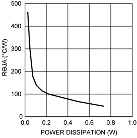 Figure 38. RθJA vs Internal Dissipation
For 5-pin SOT-23 package typical applications, RθJA numbers range from 164.2°C/W, and RθJC varies from 115.3°C/W. These values are for PCBs with two and four layer boards with 0.5 oz copper, with two to four thermal vias from GND pin to bottom layer.
Using typical thermal impedances and an ambient temperature maximum of 75°C, if the design requires more dissipation than 400 mW internal to the device, or there is 750 mW of total power loss in the application, TI recommends using the 6-pin WSON or the 8-pin MSOP-PowerPad package with the exposed DAP.
