ZHCSIR2 September 2018 LM2735-Q1
PRODUCTION DATA.
- 1 特性
- 2 应用
- 3 说明
- 4 修订历史记录
- 5 Pin Configuration and Functions
- 6 Specifications
- 7 Detailed Description
-
8 Application and Implementation
- 8.1 Application Information
- 8.2
Typical Applications
- 8.2.1 LM2735X-Q1 SOT-23 Design Example 1
- 8.2.2 LM2735Y-Q1 SOT-23 Design Example 2
- 8.2.3 LM2735X-Q1 WSON Design Example 3
- 8.2.4 LM2735Y-Q1 WSON Design Example 4
- 8.2.5 LM2735X-Q1 SOT-23 Design Example 6
- 8.2.6 LM2735Y-Q1 SOT-23 Design Example 7
- 8.2.7 LM2735X-Q1 SOT-23 Design Example 8
- 8.2.8 LM2735Y-Q1 SOT-23 Design Example 9
- 8.2.9 LM2735X-Q1 WSON Design Example 10
- 8.2.10 LM2735Y-Q1 WSON Design Example 11
- 8.2.11 LM2735X-Q1 WSON SEPIC Design Example 12
- 8.2.12 LM2735X-Q1 SOT-23 LED Design Example 14
- 8.2.13 LM2735Y-Q1 WSON FlyBack Design Example 15
- 8.2.14 LM2735X-Q1 SOT-23 LED Design Example 16 VRAIL > 5.5 V Application
- 8.2.15 LM2735X-Q1 SOT-23 LED Design Example 17 Two-Input Voltage Rail Application
- 8.2.16 SEPIC Converter
- 9 Power Supply Recommendations
- 10Layout
- 11器件和文档支持
- 12机械、封装和可订购信息
10.3.5.2 Example From Previous Calculations
PDissipation = 475 mW
TA at Shutdown = 139°C
TCase-Top at Shutdown = 155°C

RθJA WSON = 55°C/W
RψJC WSON = 21°C/W
WSON typical application produces RθJA numbers in the range of 50°C/W to 65°C/W, and RψJC varies from 18°C/W to 28°C/W. These values are for PCBs with two and four layer boards with 0.5-oz copper, and 4 to 6 thermal vias to bottom side ground plane under the DAP.
For 5-pin SOT-23 package typical applications, RθJA numbers range from 80°C/W to 110°C/W, and RψJC varies from 50°C/W to 65°C/W. These values are for PCBs with 2- and 4-layer boards with 0.5-oz copper, with 2 to 4 thermal vias from GND pin to bottom layer.
For typical thermal impedances and an ambient temperature maximum of 75°C: if the design requires more than 400 mW internal to the LM2735-Q1 be dissipated, or there is 750 mW of total power loss in the application, TI recommends using the 6-pin WSON package.
NOTE
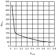
To use these procedures, it is important to dissipate an amount of power within the device to indicate a true thermal impedance value. If a very small internal dissipated value is used, it can be determined that the thermal impedance calculated is abnormally high, and subject to error. Figure 48 shows the nonlinear relationship of internal power dissipation vs RθJA.
 Figure 48. RθJA vs Internal Dissipation for the WSON