ZHCSIR2 September 2018 LM2735-Q1
PRODUCTION DATA.
- 1 特性
- 2 应用
- 3 说明
- 4 修订历史记录
- 5 Pin Configuration and Functions
- 6 Specifications
- 7 Detailed Description
-
8 Application and Implementation
- 8.1 Application Information
- 8.2
Typical Applications
- 8.2.1 LM2735X-Q1 SOT-23 Design Example 1
- 8.2.2 LM2735Y-Q1 SOT-23 Design Example 2
- 8.2.3 LM2735X-Q1 WSON Design Example 3
- 8.2.4 LM2735Y-Q1 WSON Design Example 4
- 8.2.5 LM2735X-Q1 SOT-23 Design Example 6
- 8.2.6 LM2735Y-Q1 SOT-23 Design Example 7
- 8.2.7 LM2735X-Q1 SOT-23 Design Example 8
- 8.2.8 LM2735Y-Q1 SOT-23 Design Example 9
- 8.2.9 LM2735X-Q1 WSON Design Example 10
- 8.2.10 LM2735Y-Q1 WSON Design Example 11
- 8.2.11 LM2735X-Q1 WSON SEPIC Design Example 12
- 8.2.12 LM2735X-Q1 SOT-23 LED Design Example 14
- 8.2.13 LM2735Y-Q1 WSON FlyBack Design Example 15
- 8.2.14 LM2735X-Q1 SOT-23 LED Design Example 16 VRAIL > 5.5 V Application
- 8.2.15 LM2735X-Q1 SOT-23 LED Design Example 17 Two-Input Voltage Rail Application
- 8.2.16 SEPIC Converter
- 9 Power Supply Recommendations
- 10Layout
- 11器件和文档支持
- 12机械、封装和可订购信息
8.2.16.1.2 Small Ripple Approximation
In a well-designed SEPIC converter, the output voltage, input voltage ripple, and inductor ripple is small in comparison to the DC magnitude. Therefore, it is a safe approximation to assume a DC value for these components. The main objective of the Steady State Analysis is to determine the steady state duty-cycle, voltage and current stresses on all components, and proper values for all components.
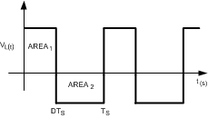
In a steady-state converter, the net volt-seconds across an inductor after one cycle equals zero. Also, the charge into a capacitor equals the charge out of a capacitor in one cycle.
Therefore:

Substituting IL1 into IL2

The average inductor current of L2 is the average output load.
 Figure 38. Inductor Volt-Sec Balance Waveform
 Applying charge balance on C1:

Since there are no DC voltages across either inductor, and capacitor C6 is connected to VIN through L1 at one end, or to ground through L2 on the other end, we can say that
Therefore:

This verifies the original conversion ratio equation.
It is important to remember that the internal switch current is equal to IL1 and IL2. During the D interval. Design the converter so that the minimum specified peak switch current limit (2.1 A) is not exceeded.