ZHCSKZ6A March 2020 – August 2020 LM25184
PRODUCTION DATA
- 1 特性
- 2 应用
- 3 说明
- 4 Revision History
- 5 Pin Configuration and Functions
- 6 Specifications
-
7 Detailed Description
- 7.1 Overview
- 7.2 Functional Block Diagram
- 7.3
Feature Description
- 7.3.1 Integrated Power MOSFET
- 7.3.2 PSR Flyback Modes of Operation
- 7.3.3 Setting the Output Voltage
- 7.3.4 Control Loop Error Amplifier
- 7.3.5 Precision Enable
- 7.3.6 Configurable Soft Start
- 7.3.7 External Bias Supply
- 7.3.8 Minimum On-Time and Off-Time
- 7.3.9 Overcurrent Protection
- 7.3.10 Thermal Shutdown
- 7.4 Device Functional Modes
-
8 Application and Implementation
- 8.1 Application Information
- 8.2
Typical Applications
- 8.2.1
Design 1: Wide VIN, Low IQ PSR Flyback Converter Rated at 12 V, 1 A
- 8.2.1.1 Design Requirements
- 8.2.1.2
Detailed Design Procedure
- 8.2.1.2.1 Custom Design With WEBENCH® Tools
- 8.2.1.2.2 Custom Design With Excel Quickstart Tool
- 8.2.1.2.3 Flyback Transformer – T1
- 8.2.1.2.4 Flyback Diode – DFLY
- 8.2.1.2.5 Leakgae Inductance Clamp Circuit – DF, DCLAMP
- 8.2.1.2.6 Output Capacitor – COUT
- 8.2.1.2.7 Input Capacitor – CIN
- 8.2.1.2.8 Feedback Resistor – RFB
- 8.2.1.2.9 Thermal Compensation Resistor – RTC
- 8.2.1.2.10 UVLO Resistors – RUV1, RUV2
- 8.2.1.2.11 Soft-Start Capacitor – CSS
- 8.2.2 Application Curves
- 8.2.3 Design 2: PSR Flyback Converter With Dual Outputs of 15 V and –8 V at 0.5 A
- 8.2.1
Design 1: Wide VIN, Low IQ PSR Flyback Converter Rated at 12 V, 1 A
- 9 Power Supply Recommendations
- 10Layout
- 11Device and Documentation Support
- 12Mechanical, Packaging, and Orderable Information
8.2.1.2.3 Flyback Transformer – T1
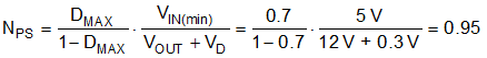
Choose a turns ratio of 1 : 1 based on an approximate 70% max duty cycle at minimum input voltage using Equation 14, rounding up or down as needed. While the maximum duty cycle can approach 80% if a particularly wide input voltage application is needed, it increases the peak current stress of the secondary-side components.
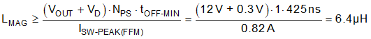
Select a magnetizing inductance based on the minimum off-time constraint using Equation 15. Choose a value of 7 µH to allow some margin for this application. Specify a saturation current of 5 A, above the maximum switch current specification of the LM25184.
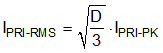
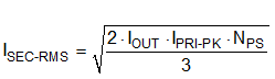
Note that a higher magnetizing inductance provides a larger operating range for BCM and FFM, but the leakage inductance can increase based on a higher number of primary turns, NP. Equation 16 and Equation 17 give the primary and secondary winding RMS currents, respectively.
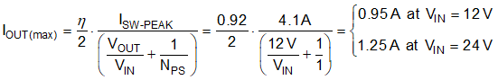
Find the maximum output current for a given turns ratio using Equation 18, where η is the efficiency and the typical value for ISW-PEAK is the 4.1-A switch peak current threshold. Iterate by increasing the turns ratio if the output current capability is too low at minimum input voltage, checking that the SW voltage rating of 65 V is not exceeded at maximum input voltage.