ZHCSKZ6A March 2020 – August 2020 LM25184
PRODUCTION DATA
- 1 特性
- 2 应用
- 3 说明
- 4 Revision History
- 5 Pin Configuration and Functions
- 6 Specifications
-
7 Detailed Description
- 7.1 Overview
- 7.2 Functional Block Diagram
- 7.3
Feature Description
- 7.3.1 Integrated Power MOSFET
- 7.3.2 PSR Flyback Modes of Operation
- 7.3.3 Setting the Output Voltage
- 7.3.4 Control Loop Error Amplifier
- 7.3.5 Precision Enable
- 7.3.6 Configurable Soft Start
- 7.3.7 External Bias Supply
- 7.3.8 Minimum On-Time and Off-Time
- 7.3.9 Overcurrent Protection
- 7.3.10 Thermal Shutdown
- 7.4 Device Functional Modes
-
8 Application and Implementation
- 8.1 Application Information
- 8.2
Typical Applications
- 8.2.1
Design 1: Wide VIN, Low IQ PSR Flyback Converter Rated at 12 V, 1 A
- 8.2.1.1 Design Requirements
- 8.2.1.2
Detailed Design Procedure
- 8.2.1.2.1 Custom Design With WEBENCH® Tools
- 8.2.1.2.2 Custom Design With Excel Quickstart Tool
- 8.2.1.2.3 Flyback Transformer – T1
- 8.2.1.2.4 Flyback Diode – DFLY
- 8.2.1.2.5 Leakgae Inductance Clamp Circuit – DF, DCLAMP
- 8.2.1.2.6 Output Capacitor – COUT
- 8.2.1.2.7 Input Capacitor – CIN
- 8.2.1.2.8 Feedback Resistor – RFB
- 8.2.1.2.9 Thermal Compensation Resistor – RTC
- 8.2.1.2.10 UVLO Resistors – RUV1, RUV2
- 8.2.1.2.11 Soft-Start Capacitor – CSS
- 8.2.2 Application Curves
- 8.2.3 Design 2: PSR Flyback Converter With Dual Outputs of 15 V and –8 V at 0.5 A
- 8.2.1
Design 1: Wide VIN, Low IQ PSR Flyback Converter Rated at 12 V, 1 A
- 9 Power Supply Recommendations
- 10Layout
- 11Device and Documentation Support
- 12Mechanical, Packaging, and Orderable Information
7.3.5 Precision Enable
The precision EN/UVLO input supports adjustable input undervoltage lockout (UVLO) with hysteresis for application specific power-up and power-down requirements. EN/UVLO connects to a comparator with a 1.5-V reference voltage and 50-mV hysteresis. An external logic signal can be used to drive the EN/UVLO input to toggle the output on and off for system sequencing or protection. The simplest way to enable the LM25184 is to connect EN/UVLO directly to VIN. This allows the LM25184 to start up when VIN is within its valid operating range. However, many applications benefit from using resistor divider RUV1 and RUV2 as shown in Figure 7-3 to establish a precision UVLO level.
 Figure 7-3 Programmable Input Voltage
UVLO With Hysteresis
Figure 7-3 Programmable Input Voltage
UVLO With HysteresisUse Equation 10 and Equation 11 to calculate the input UVLO voltages turnon and turnoff voltages, respectively.
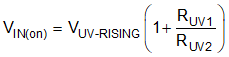
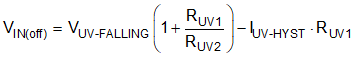
where
- VUV-RISING and VUV-FALLING are the UVLO comparator thresholds
- IUV-HYST is the hysteresis current
The LM25184 also provides a low-IQ shutdown mode when the EN/UVLO voltage is pulled below a base-emitter voltage drop (approximately 0.6 V at room temperature). If the EN/UVLO voltage is below this hard shutdown threshold, the internal LDO regulator powers off, and the internal bias-supply rail collapses, shutting down the bias currents of the LM25184. The LM25184 operates in standby mode when the EN/UVLO voltage is between the hard shutdown and precision-enable thresholds.