ZHCSE44C august 2015 – may 2023 ISO5852S
PRODUCTION DATA
- 1
- 1 特性
- 2 应用
- 3 说明
- 4 Revision History
- 5 说明(续)
- 6 Pin Configuration and Function
-
7 Specifications
- 7.1 Absolute Maximum Ratings
- 7.2 ESD Ratings
- 7.3 Recommended Operating Conditions
- 7.4 Thermal Information
- 7.5 Power Ratings
- 7.6 Insulation Specifications
- 7.7 Safety-Related Certifications
- 7.8 Safety Limiting Values
- 7.9 Electrical Characteristics
- 7.10 Switching Characteristics
- 7.11 Insulation Characteristics Curves
- 7.12 Typical Characteristics
- 8 Parameter Measurement Information
- 9 Detailed Description
-
10Application and Implementation
- 10.1 Application Information
- 10.2
Typical Applications
- 10.2.1 Design Requirements
- 10.2.2
Detailed Design Procedure
- 10.2.2.1 Recommended ISO5852S Application Circuit
- 10.2.2.2 FLT and RDY Pin Circuitry
- 10.2.2.3 Driving the Control Inputs
- 10.2.2.4 Local Shutdown and Reset
- 10.2.2.5 Global-Shutdown and Reset
- 10.2.2.6 Auto-Reset
- 10.2.2.7 DESAT Pin Protection
- 10.2.2.8 DESAT Diode and DESAT Threshold
- 10.2.2.9 Determining the Maximum Available, Dynamic Output Power, POD-max
- 10.2.2.10 Example
- 10.2.2.11 Higher Output Current Using an External Current Buffer
- 10.2.3 Application Curves
- 11Power Supply Recommendations
- 12Layout
- 13Device and Documentation Support
- 14Mechanical, Packaging, and Orderable Information
10.2.2.9 Determining the Maximum Available, Dynamic Output Power, POD-max
The ISO5852S maximum-allowed total power consumption of PD = 251 mW consists of the total input power, PID, the total output power, POD, and the output power under load, POL:
Equation 1. PD = PID + POD + POL
With:
Equation 2. PID = VCC1-max × ICC1-max = 5.5 V × 4.5 mA = 24.75 mW
and:
Equation 3. POD = (VCC2 – VEE2) × ICC2-max = (15 V – [–8 V]) × 6 mA = 138 mW
then:
Equation 4. POL = PD – PID – POD = 251 mW – 24.75 mW – 138 mW = 88.25 mW
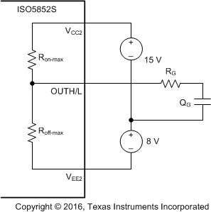
In comparison to POL, the actual dynamic output power under worst case condition, POL-WC, depends on a variety of parameters:
Equation 5. 

where
- fINP = signal frequency at the control input IN+
- QG = power device gate charge
- VCC2 = positive output supply with respect to GND2
- VEE2 = negative output supply with respect to GND2
- ron-max = worst case output resistance in the on-state: 4 Ω
- roff-max = worst case output resistance in the off-state: 2.5 Ω
- RG = gate resistor
When RG is determined, Equation 5 is to be used to verify whether POL-WC < POL. Figure 10-9 shows a simplified output stage model for calculating POL-WC.
 Figure 10-9 Simplified Output Model for Calculating POL-WC