ZHCSE44C august 2015 – may 2023 ISO5852S
PRODUCTION DATA
- 1
- 1 特性
- 2 应用
- 3 说明
- 4 Revision History
- 5 说明(续)
- 6 Pin Configuration and Function
-
7 Specifications
- 7.1 Absolute Maximum Ratings
- 7.2 ESD Ratings
- 7.3 Recommended Operating Conditions
- 7.4 Thermal Information
- 7.5 Power Ratings
- 7.6 Insulation Specifications
- 7.7 Safety-Related Certifications
- 7.8 Safety Limiting Values
- 7.9 Electrical Characteristics
- 7.10 Switching Characteristics
- 7.11 Insulation Characteristics Curves
- 7.12 Typical Characteristics
- 8 Parameter Measurement Information
- 9 Detailed Description
-
10Application and Implementation
- 10.1 Application Information
- 10.2
Typical Applications
- 10.2.1 Design Requirements
- 10.2.2
Detailed Design Procedure
- 10.2.2.1 Recommended ISO5852S Application Circuit
- 10.2.2.2 FLT and RDY Pin Circuitry
- 10.2.2.3 Driving the Control Inputs
- 10.2.2.4 Local Shutdown and Reset
- 10.2.2.5 Global-Shutdown and Reset
- 10.2.2.6 Auto-Reset
- 10.2.2.7 DESAT Pin Protection
- 10.2.2.8 DESAT Diode and DESAT Threshold
- 10.2.2.9 Determining the Maximum Available, Dynamic Output Power, POD-max
- 10.2.2.10 Example
- 10.2.2.11 Higher Output Current Using an External Current Buffer
- 10.2.3 Application Curves
- 11Power Supply Recommendations
- 12Layout
- 13Device and Documentation Support
- 14Mechanical, Packaging, and Orderable Information
10.2.2.11 Higher Output Current Using an External Current Buffer
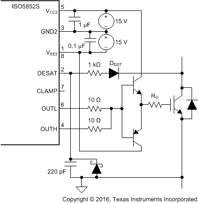
To increase the IGBT gate drive current, a non-inverting current buffer (such as the npn/pnp buffer shown in Figure 10-10) can be used. Inverting types are not compatible with the desaturation fault protection circuitry and must be avoided. The MJD44H11/MJD45H11 pair is appropriate for currents up to 8 A, the D44VH10/ D45VH10 pair for up to 15 A maximum.
 Figure 10-10 Current Buffer for Increased Drive Current