ZHCSIX9B october   2018  – october 2020 ISO1042-Q1

PRODUCTION DATA  

  1.   1
  2. 特性
  3. 应用
  4. 说明
  5. Revision History
  6. Pin Configuration and Functions
  7. Specifications
    1. 6.1  Absolute Maximum Ratings
    2. 6.2  ESD Ratings
    3. 6.3  Transient Immunity
    4. 6.4  Recommended Operating Conditions
    5. 6.5  Thermal Information
    6. 6.6  Power Ratings
    7. 6.7  Insulation Specifications
    8. 6.8  Safety-Related Certifications
    9. 6.9  Safety Limiting Values
    10. 6.10 Electrical Characteristics - DC Specification
    11. 6.11 Switching Characteristics
    12. 6.12 Insulation Characteristics Curves
    13. 6.13 Typical Characteristics
  8. Parameter Measurement Information
    1. 7.1 Test Circuits
  9. Detailed Description
    1. 8.1 Overview
    2. 8.2 Functional Block Diagram
    3. 8.3 Feature Description
      1. 8.3.1 CAN Bus States
      2. 8.3.2 Digital Inputs and Outputs: TXD (Input) and RXD (Output)
      3. 8.3.3 Protection Features
        1. 8.3.3.1 TXD Dominant Timeout (DTO)
        2. 8.3.3.2 Thermal Shutdown (TSD)
        3. 8.3.3.3 Undervoltage Lockout and Default State
        4. 8.3.3.4 Floating Pins
        5. 8.3.3.5 Unpowered Device
        6. 8.3.3.6 CAN Bus Short Circuit Current Limiting
    4. 8.4 Device Functional Modes
  10. Application and Implementation
    1. 9.1 Application Information
    2. 9.2 Typical Application
      1. 9.2.1 Design Requirements
      2. 9.2.2 Detailed Design Procedure
        1. 9.2.2.1 Bus Loading, Length and Number of Nodes
        2. 9.2.2.2 CAN Termination
      3. 9.2.3 Application Curve
  11. 10Power Supply Recommendations
  12. 11Layout
    1. 11.1 Layout Guidelines
      1. 11.1.1 PCB Material
    2. 11.2 Layout Example
  13. 12Device and Documentation Support
    1. 12.1 Documentation Support
      1. 12.1.1 Related Documentation
    2. 12.2 Receiving Notification of Documentation Updates
    3. 12.3 支持资源
    4. 12.4 Trademarks
    5. 12.5 静电放电警告
    6. 12.6 术语表
  14. 13Mechanical, Packaging, and Orderable Information

封装选项

机械数据 (封装 | 引脚)
散热焊盘机械数据 (封装 | 引脚)
订购信息

Typical Characteristics

GUID-8972DB20-F054-488A-9A63-B3F28BE78F2A-low.gif
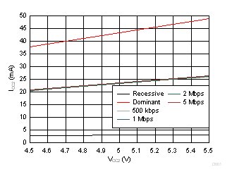
VCC1 = 5 VRL = 60 ΩCL(RXD) = 15 pF
Temp = 25°C
Figure 6-5 ICC2 vs VCC2 for Recessive, Dominant and Different CAN Datarates
GUID-DD42634C-AAB1-42C1-B91F-560102C9A2EF-low.gif
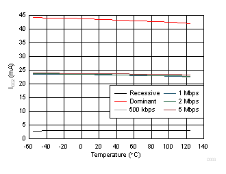
VCC1 = VCC2 = 5 VRL = 60 ΩCL(RXD) = 15 pF
Figure 6-7 ICC2 vs Ambient Temperature for Recessive, Dominant and Different CAN Datarates
GUID-2F8E464F-94C3-47D2-AE45-F140616E625A-low.gif
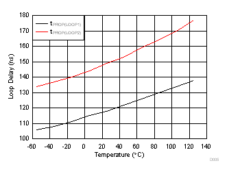
VCC1 = VCC2 = 5 VRL = 60 ΩCL(RXD) = 15 pF
Figure 6-9 Loop Delay vs Ambient Temperature
GUID-EB3C976E-3875-462F-89A4-20C385C206EC-low.gif
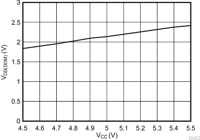
VCC1 = 5 VRL = 60 Ω
CL = OpenTemp = 25°C
Figure 6-11 VOD(DOM) Over VCC
GUID-245A7461-BA71-4B99-8653-DC1E493187F2-low.png
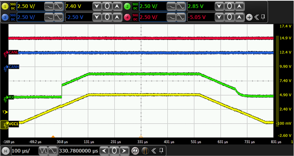
TXD = VCC1RL = 60 ΩVCC1 = VCC2 = 5 V
Figure 6-13 Glitch Free Power Up on VCC1 – CAN Bus Remains Recessive
GUID-B4E251CF-B059-4ADC-93C8-DF9109088C04-low.gif
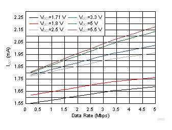
VCC2 = 5 VRL = 60 ΩCL(RXD) = 15 pF
Temp = 25°C
Figure 6-6 ICC1 vs Datarate
GUID-9CFBBC47-B0E4-40A3-94FA-C9B004AE43B2-low.gif
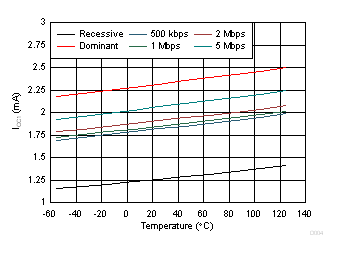
VCC1 = VCC2 = 5 VRL = 60 ΩCL(RXD) = 15 pF
Temp = 25°C
Figure 6-8 : ICC1 vs Ambient Temperature for Recessive, Dominant and Different CAN Datarates.
GUID-C4892C45-E2E1-4809-906B-AFD64521F89D-low.gif
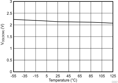
VCC = 5 VVCC1 = 5 VRL = 60 Ω
CL = Open
Figure 6-10 VOD(DOM) Over Temperature
GUID-EE72C4B8-3DA2-4DD5-B6B1-B3BD29DAADCA-low.png
VCC1 = VCC2 = 5 VRL = 60 ΩCL = 100 pF
CL(RXD) = 15 pF
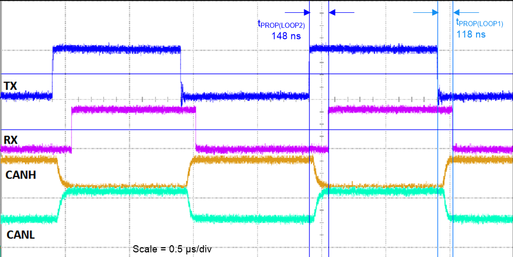
Figure 6-12 Typical TXD, RXD, CANH and CANL Waveforms at 1 Mbps
GUID-3D1D9C44-C527-49B1-AAB8-368C5441294C-low.png
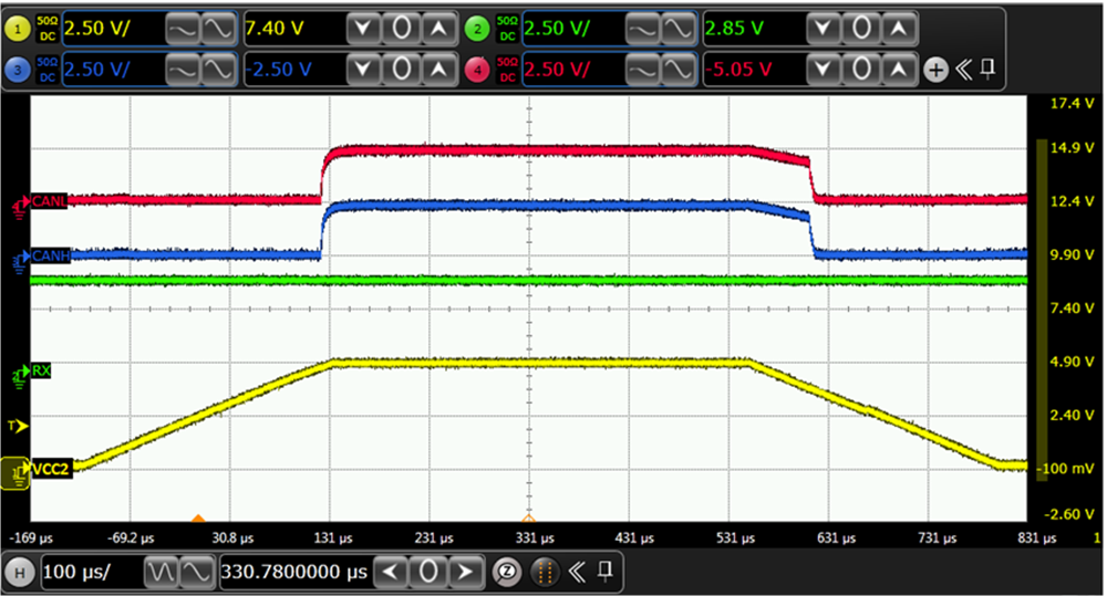
TXD = VCC1RL = 60 ΩVCC1 = VCC2 = 5 V
Figure 6-14 Glitch Free Power Up on VCC2 – CAN Bus Remains Recessive