ZHCSH47 November   2017 INA317

PRODUCTION DATA.  

  1. 特性
  2. 应用
  3. 说明
    1.     Device Images
      1.      简化原理图
  4. 修订历史记录
  5. Pin Configuration and Functions
    1.     Pin Functions
  6. Specifications
    1. 6.1 Absolute Maximum Ratings
    2. 6.2 ESD Ratings
    3. 6.3 Recommended Operating Conditions
    4. 6.4 Thermal Information
    5. 6.5 Electrical Characteristics
    6. 6.6 Typical Characteristics
  7. Detailed Description
    1. 7.1 Overview
    2. 7.2 Functional Block Diagram
    3. 7.3 Feature Description
    4. 7.4 Device Functional Modes
      1. 7.4.1 Internal Offset Correction
      2. 7.4.2 Input Common-Mode Range
  8. Application and Implementation
    1. 8.1 Application Information
    2. 8.2 Typical Application
      1. 8.2.1 Design Requirements
      2. 8.2.2 Detailed Design Procedure
        1. 8.2.2.1  Setting the Gain
        2. 8.2.2.2  Internal Offset Correction
        3. 8.2.2.3  Offset Trimming
        4. 8.2.2.4  Noise Performance
        5. 8.2.2.5  Input Bias Current Return Path
        6. 8.2.2.6  Input Common-Mode Range
        7. 8.2.2.7  Operating Voltage
        8. 8.2.2.8  Low Voltage Operation
        9. 8.2.2.9  Single-Supply Operation
        10. 8.2.2.10 Input Protection
      3. 8.2.3 Application Curves
  9. Power Supply Recommendations
  10. 10Layout
    1. 10.1 Layout Guidelines
    2. 10.2 Layout Example
  11. 11器件和文档支持
    1. 11.1 器件支持
      1. 11.1.1 开发支持
        1. 11.1.1.1 TINA-TI(免费下载软件)
    2. 11.2 文档支持
      1. 11.2.1 相关文档
    3. 11.3 商标
    4. 11.4 静电放电警告
    5. 11.5 Glossary
  12. 12机械、封装和可订购信息

封装选项

机械数据 (封装 | 引脚)
散热焊盘机械数据 (封装 | 引脚)
订购信息

Single-Supply Operation

The INA317 device can be used on single power supplies of 1.8 V to 5.5 V. Figure 35 shows a basic single-supply circuit. The output REF pin is connected to midsupply. Zero differential input voltage demands an output voltage of midsupply. Actual output voltage swing is limited to approximately 50 mV more than ground when the load is referred to ground as shown. Figure 29 shows how the output voltage swing varies with output current.

With single-supply operation, VIN+ and VIN– must be 0.1 V more than ground for linear operation. For instance, the inverting input cannot connect to ground to measure a voltage that is connected to the noninverting input.

To show the issues affecting low voltage operation, see Figure 35. Figure 35 shows the INA317 device operating from a single 3-V supply. A resistor in series with the low side of the bridge ensures that the bridge output voltage is within the common-mode range of the amplifier inputs.
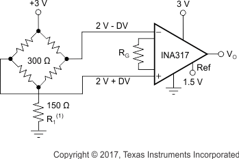
INA317 ai_1sup_bridge_bos445.gif
R1 creates proper common-mode voltage only for low-voltage operation; see Single-Supply Operation.
Figure 35. Single-Supply Bridge Amplifier