ZHCSH47 November   2017 INA317

PRODUCTION DATA.  

  1. 特性
  2. 应用
  3. 说明
    1.     Device Images
      1.      简化原理图
  4. 修订历史记录
  5. Pin Configuration and Functions
    1.     Pin Functions
  6. Specifications
    1. 6.1 Absolute Maximum Ratings
    2. 6.2 ESD Ratings
    3. 6.3 Recommended Operating Conditions
    4. 6.4 Thermal Information
    5. 6.5 Electrical Characteristics
    6. 6.6 Typical Characteristics
  7. Detailed Description
    1. 7.1 Overview
    2. 7.2 Functional Block Diagram
    3. 7.3 Feature Description
    4. 7.4 Device Functional Modes
      1. 7.4.1 Internal Offset Correction
      2. 7.4.2 Input Common-Mode Range
  8. Application and Implementation
    1. 8.1 Application Information
    2. 8.2 Typical Application
      1. 8.2.1 Design Requirements
      2. 8.2.2 Detailed Design Procedure
        1. 8.2.2.1  Setting the Gain
        2. 8.2.2.2  Internal Offset Correction
        3. 8.2.2.3  Offset Trimming
        4. 8.2.2.4  Noise Performance
        5. 8.2.2.5  Input Bias Current Return Path
        6. 8.2.2.6  Input Common-Mode Range
        7. 8.2.2.7  Operating Voltage
        8. 8.2.2.8  Low Voltage Operation
        9. 8.2.2.9  Single-Supply Operation
        10. 8.2.2.10 Input Protection
      3. 8.2.3 Application Curves
  9. Power Supply Recommendations
  10. 10Layout
    1. 10.1 Layout Guidelines
    2. 10.2 Layout Example
  11. 11器件和文档支持
    1. 11.1 器件支持
      1. 11.1.1 开发支持
        1. 11.1.1.1 TINA-TI(免费下载软件)
    2. 11.2 文档支持
      1. 11.2.1 相关文档
    3. 11.3 商标
    4. 11.4 静电放电警告
    5. 11.5 Glossary
  12. 12机械、封装和可订购信息

封装选项

机械数据 (封装 | 引脚)
散热焊盘机械数据 (封装 | 引脚)
订购信息

Typical Characteristics

at TA = 25°C, VS = 5 V, RL = 10 kΩ, VREF = midsupply, and G = 1, (unless otherwise noted)
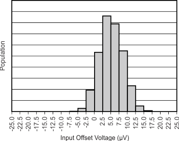
INA317 tc_histo_in_vo_bos445.gif
VS = 5.5 V
Figure 1. Input Offset Voltage
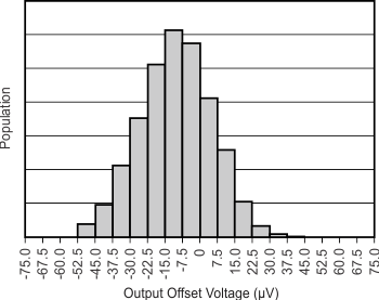
INA317 tc_histo_out_off_bos445.gif
VS = 5.5 V
Figure 3. Output Offset Voltage
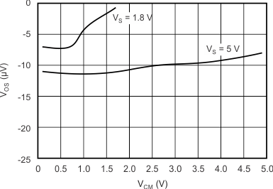
INA317 tc_vos-vcm_bos445.gif
Figure 5. Offset Voltage vs Common-Mode Voltage
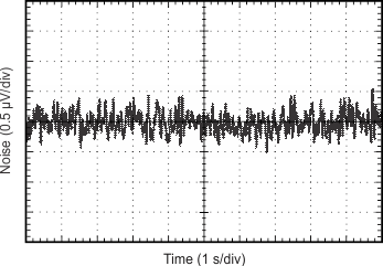
INA317 tc_noise_100g_bos445.gif
Gain = 100
Figure 7. 0.1-Hz to 10-Hz Noise
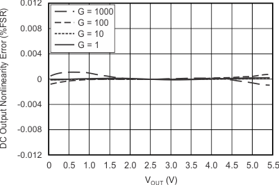
INA317 tc_inl_err_bos445.gif
VS = ±2.75 V
Figure 9. Nonlinearity Error
INA317 tc_lg_resp_100g_bos445.gif
Gain = 100
Figure 11. Large-Signal Step Response
INA317 tc_sm_resp_100g_bos445.gif
Gain = 100
Figure 13. Small-Signal Step Response
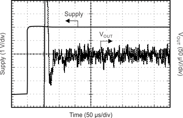
INA317 tc_startup_tset_bos445.gif
Gain = 1
Figure 15. Start-Up Settling Time
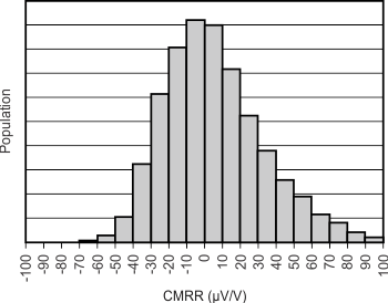
INA317 tc_histo_cmrr_1g_bos445.gif
VS = 5.5 V
Figure 17. Common-Mode Rejection Ratio
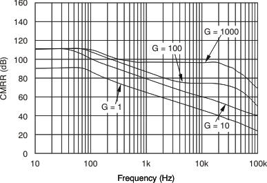
INA317 tc_cmrr-frq_bos445.gif
Figure 19. Common-Mode Rejection Ratio vs Frequency
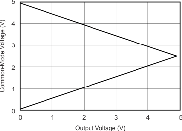
INA317 tc_typ_cmr-vo_tri_bos445.gif
VS = 5 V VREF = 0 All gains
Figure 21. Typical Common-Mode Range vs Output Voltage
INA317 tc_typ_cmr-vo_tri_1p8_bos445.gif
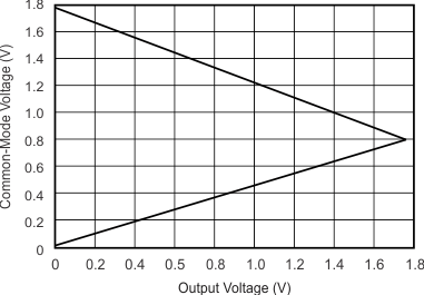
VS = 1.8 V VREF = 0
Figure 23. Typical Common-Mode Range vs Output Voltage
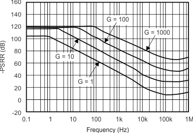
INA317 tc_neg_psrr-frq_bos445.gif
VS = 5 V
Figure 25. Negative Power-Supply Rejection Ratio
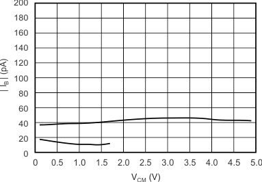
INA317 tc_in_ib-vcm_bos445.gif
VS = 5 V VS = 1.8 V
Figure 27. Input Bias Current vs Common-Mode Voltage
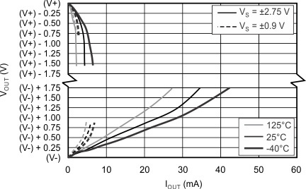
INA317 tc_vo_swing-io_bos445.gif
Figure 29. Output Voltage Swing vs Output Current
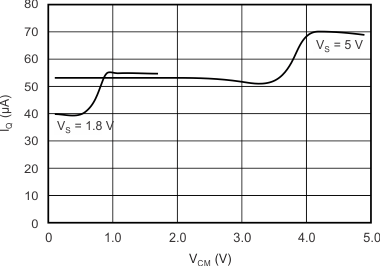
INA317 tc_iq-vcm_bos445.gif
Figure 31. Quiescent Current vs Common-Mode Voltage
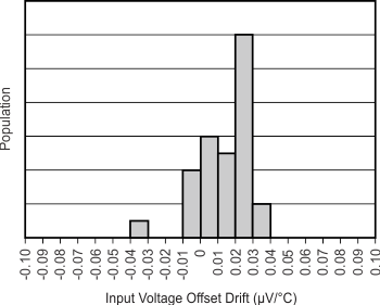
INA317 tc_histo_in_vo_drift_bos445.gif
VS = 5.5 V TA = –40°C to +125°C
Figure 2. Input Voltage Offset Drift
INA317 tc_histo_out_vo_drift_bos445.gif
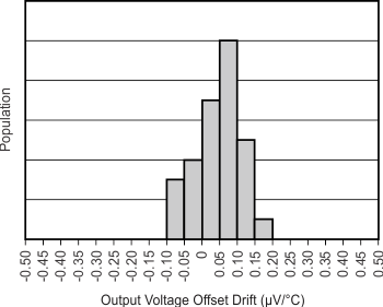
VS = 5.5 V TA = –40°C to +125°C
Figure 4. Output Voltage Offset Drift
INA317 tc_noise_1g_bos445.gif
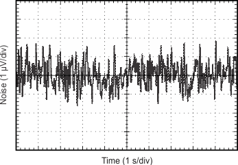
Gain = 1
Figure 6. 0.1-Hz to 10-Hz Noise
INA317 tc_noise_spec_bos445.gif
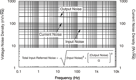
Figure 8. Spectral Noise Density
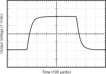
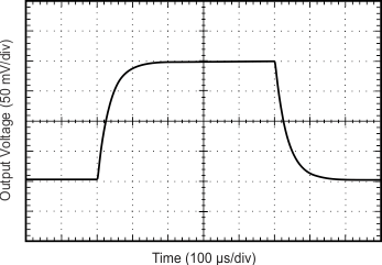
INA317 tc_lg_resp_1g_bos445.gif
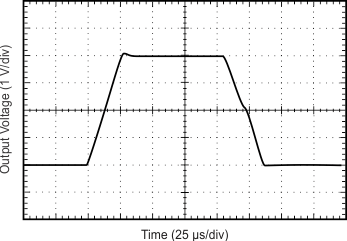
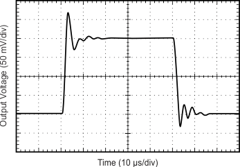
Gain = 1
Figure 10. Large Signal Response
INA317 tc_sm_resp_1g_bos445.gif
Gain = 1
Figure 12. Small-Signal Step Response
INA317 tc_tset-g_bos445.gif
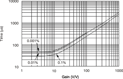
Figure 14. Settling Time vs Gain
INA317 tc_g-frq_bos445.gif
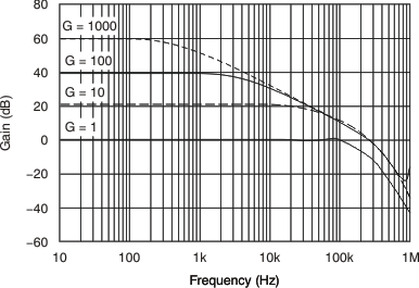
Figure 16. Gain vs Frequency
INA317 tc_cmrr-tmp_bos445.gif
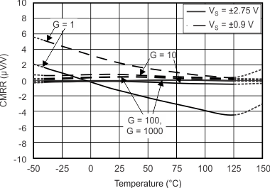
Figure 18. Common-Mode Rejection Ratio vs Temperature
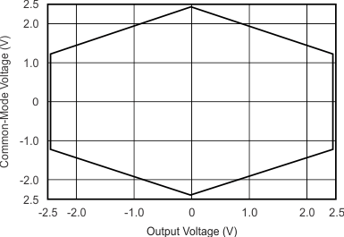
INA317 tc_typ_cmr-vo_oct_bos445.gif
VS = ±2.5 V VREF = 0 All gains
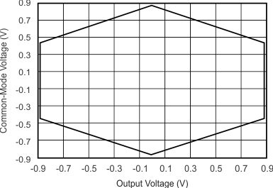
Figure 20. Typical Common-Mode Range vs Output Voltage
INA317 tc_typ_cmr-vo_oct_0p9_bos445.gif
VS = ±0.9 V VREF = 0 All gains
Figure 22. Typical Common-Mode Range vs Output Voltage
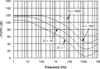
INA317 tc_pos_psrr-frq_bos445.gif
Figure 24. Positive Power-Supply Rejection Ratio
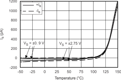
INA317 tc_in_ib-tmp_bos445.gif
Figure 26. Input Bias Current vs Temperature
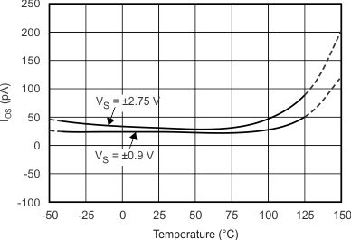
INA317 tc_in_ios-tmp_bos445.gif
Figure 28. Input Offset Current vs Temperature
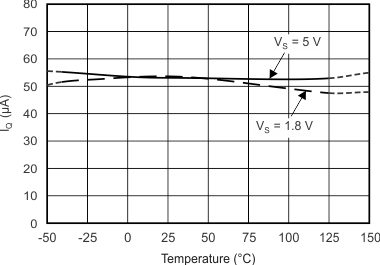
INA317 tc_iq-tmp_bos445.gif
Figure 30. Quiescent Current vs Temperature