ZHCSC53A February 2014 – March 2014 INA225
PRODUCTION DATA.
- 1 特性
- 2 应用范围
- 3 说明
- 4 修订历史记录
- 5 Terminal Configuration and Functions
- 6 Specifications
- 7 Detailed Description
- 8 Applications and Implementation
- 9 Power Supply Recommendations
- 10Layout
- 11器件和文档支持
- 12机械封装和可订购信息
8 Applications and Implementation
8.1 Application Information
The INA225 measures the voltage developed across a current-sensing resistor when current passes through it. The ability to drive the reference terminal to adjust the functionality of the output signal offers multiple configurations discussed throughout this section.
8.2 Typical Applications
8.2.1 Microcontroller-Configured Gain Selection
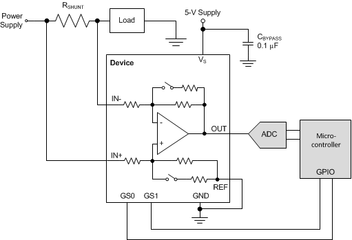 Figure 39. Microcontroller-Configured Gain Selection Schematic
8.2.1.1 Design Requirements
Figure 39 shows the typical implementation of the device interfacing with an analog-to-digital converter (ADC) and microcontroller.
8.2.1.2 Detailed Design Procedure
In this application, the device gain setting is selected and controlled by the microcontroller to ensure the device output is within the linear input range of the ADC. Because the output range of the device under a specific gain setting approaches the linear output range of the INA225 itself or the linear input range of the ADC, the microcontroller can adjust the device gain setting to ensure the signal remains within both the device and the ADC linear signal range.
8.2.1.3 Application Curve
Figure 40 illustrates how the microcontroller can monitor the ADC measurements to determine if the device gain setting should be adjusted to ensure the output of the device remains within the linear output range as well as the linear input range of the ADC. When the output of the device rises to a level near the desired maximum voltage level, the microcontroller can change the GPIO settings connected to the G0 and G1 gain-select terminals to adjust the device gain setting, thus resulting in the output voltage dropping to a lower output range. When the input current increases, the output voltage increases again to the desired maximum voltage level. The microcontroller can again change the device gain setting to drop the output voltage back to a lower range.
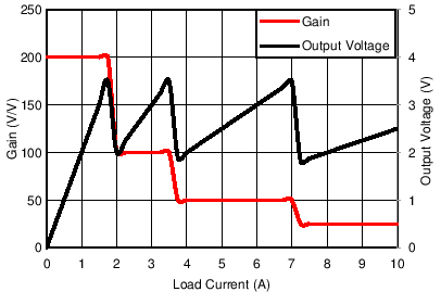 Figure 40. Microcontroller-Configured Gain Selection Response
8.2.2 Unidirectional Operation
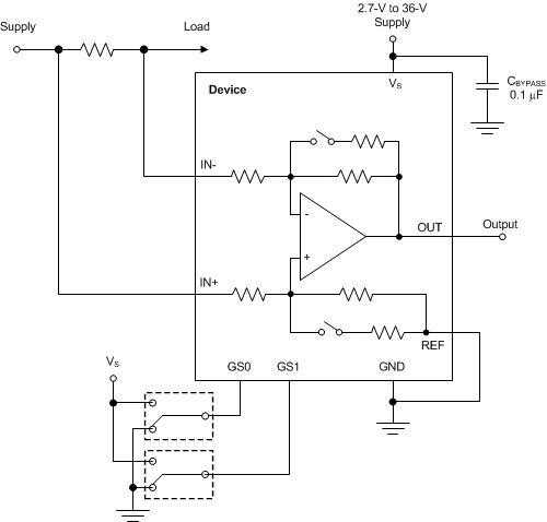 Figure 41. Unidirectional Application Schematic
8.2.2.1 Design Requirements
The device can be configured to monitor current flowing in one direction or in both directions, depending on how the REF terminal is configured. For measuring current in one direction, only the REF terminal is typically connected to ground as shown in Figure 41. With the REF terminal connected to ground, the output is low with no differential input signal applied. When the input signal increases, the output voltage at the OUT terminal increases above ground based on the device gain setting.
8.2.2.2 Detailed Design Procedure
The linear range of the output stage is limited in how close the output voltage can approach ground under zero input conditions. Resulting from an internal node limitation when the REF terminal is grounded (unidirectional configuration) the device gain setting determines how close to ground the device output voltage can achieve when no signal is applied; see Figure 14. To overcome this internal node limitation, a small reference voltage (approximately 10 mV) can be applied to the REF terminal to bias the output voltage above this voltage level. The device output swing capability returns to the 10-mV saturation level with this small reference voltage present.
At the lowest gain setting, 25 V/V, the device is capable of accurately measuring input signals that result in output voltages below this 10-mV saturation level of the output stage. For these gain settings, a reference voltage can be applied to bias the output voltage above this lower saturation level to allow the device to monitor these smaller input signals. To avoid common-mode rejection errors, buffer the reference voltage connected to the REF terminal.
A less frequently-used output biasing method is to connect the REF terminal to the supply voltage, VS. This method results in the output voltage saturating at 200 mV below the supply voltage when no differential input signal is present. This method is similar to the output saturated low condition with no input signal when the REF terminal is connected to ground. The output voltage in this configuration only responds to negative currents that develop negative differential input voltage relative to the device IN– terminal. Under these conditions, when the differential input signal increases negatively, the output voltage moves downward from the saturated supply voltage. The voltage applied to the REF terminal must not exceed the device supply voltage.
8.2.2.3 Application Curve
An example output response of a unidirectional configuration is shown in Figure 42. With the REF terminal connected directly to ground, the output voltage is biased to this zero output level. The output rises above the reference voltage for positive differential input signals but cannot fall below the reference voltage for negative differential input signals because of the grounded reference voltage.
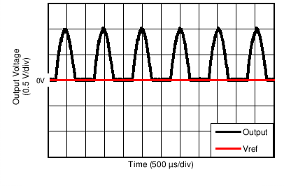 Figure 42. Unidirectional Application Output Response
8.2.3 Bidirectional Operation
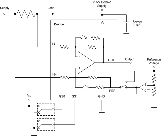 Figure 43. Bidirectional Application Schematic
8.2.3.1 Design Requirements
The device is a bidirectional, current-sense amplifier capable of measuring currents through a resistive shunt in two directions. This bidirectional monitoring is common in applications that include charging and discharging operations where the current flow-through resistor can change directions.
8.2.3.2 Detailed Design Procedure
The ability to measure this current flowing in both directions is enabled by applying a voltage to the REF terminal, as shown in Figure 43. The voltage applied to REF (VREF) sets the output state that corresponds to the zero-input level state. The output then responds by increasing above VREF for positive differential signals (relative to the IN– terminal) and responds by decreasing below VREF for negative differential signals. This reference voltage applied to the REF terminal can be set anywhere between 0 V to VS. For bidirectional applications, VREF is typically set at mid-scale for equal range in both directions. In some cases, however, VREF is set at a voltage other than half-scale when the bidirectional current is non-symmetrical.
8.2.3.3 Application Curve
An example output response of a bidirectional configuration is shown in Figure 44. With the REF terminal connected to a reference voltage, 2.5 V in this case, the output voltage is biased upwards by this reference level. The output rises above the reference voltage for positive differential input signals and falls below the reference voltage for negative differential input signals.
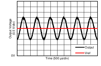 Figure 44. Bidirectional Application Output Response