ZHCSC53A February 2014 – March 2014 INA225
PRODUCTION DATA.
- 1 特性
- 2 应用范围
- 3 说明
- 4 修订历史记录
- 5 Terminal Configuration and Functions
- 6 Specifications
- 7 Detailed Description
- 8 Applications and Implementation
- 9 Power Supply Recommendations
- 10Layout
- 11器件和文档支持
- 12机械封装和可订购信息
7 Detailed Description
7.1 Overview
The INA225 is a 36-V, common-mode, zero-drift topology, current-sensing amplifier. This device features a significantly higher signal bandwidth than most comparable precision, current-sensing amplifiers, reaching up to 125 kHz at a gain of 100 V/V. A very useful feature present in the device is the built-in programmable gain selection. To increase design flexibility with the device, a programmable gain feature is added that allows changing device gain during operation in order to accurately monitor wider dynamic input signal ranges. Four discrete gain levels (25 V/V, 50 V/V, 100 V/V, and 200 V/V) are available in the device and are selected using the two gain-select terminals, GS0 and GS1.
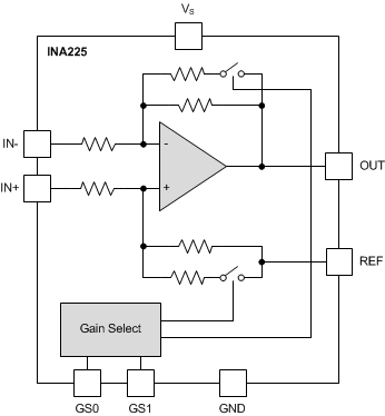
7.2 Functional Block Diagram
7.3 Feature Description
7.3.1 Selecting A Shunt Resistor
The device measures the differential voltage developed across a resistor when current flows through it. This resistor is commonly referred to as a current-sensing resistor or a current-shunt resistor, with each term commonly used interchangeably. The flexible design of the device allows a wide range of input signals to be measured across this current-sensing resistor.
Selecting the value of this current-sensing resistor is based primarily on two factors: the required accuracy of the current measurement and the allowable power dissipation across the resistor. The larger the voltage developed across this resistor the more accurate of a measurement that can be made because of the fixed internal amplifier errors. These fixed internal amplifier errors, which are dominated by the internal offset voltage of the device, result in a larger measurement uncertainty when the input signal gets smaller. When the input signal gets larger, the measurement uncertainty is reduced because the fixed errors become a smaller percentage of the signal being measured.
A system design trade-off for improving the measurement accuracy through the use of the larger input signals is the increase in the power dissipated across the current-sensing resistor. Increasing the value of the current-shunt resistor increases the differential voltage developed across the resistor when current passes through it. However, the power that is then dissipated across this component also increases. Decreasing the value of the current-shunt resistor value reduces the power dissipation requirements of the resistor, but increases the measurement errors resulting from the decreasing input signal. Finding the optimal value for the shunt resistor requires factoring both the accuracy requirement of the application and allowable power dissipation into the selection of the component. An increasing amount of very low ohmic value resistors are becoming available with values reaching down to 200 μΩ with power dissipations of up to 5 W, thus enabling very large currents to be accurately monitored using sensing resistors.
The maximum value for the current-sensing resistor that can be chosen is based on the full-scale current to be measured, the full-scale input range of the circuitry following the device, and the device gain selected. The minimum value for the current-sensing resistor is typically a design-based decision because maximizing the input range of the circuitry following the device is commonly preferred. Full-scale output signals that are significantly less than the full input range of the circuitry following the device output can limit the ability of the system to exercise the full dynamic range of system control based on the current measurement.
7.3.1.1 Selecting A Current-Sense Resistor Example
The example in Table 1 is based on a set of application characteristics, including a 10-A full-scale current range and a 4-V full-scale output requirement. The calculations for selecting a current-sensing resistor of an appropriate value are shown in Table 1.
Table 1. Calculating the Current-Sense Resistor, RSENSE
| PARAMETER | EQUATION | RESULT | |
|---|---|---|---|
| IMAX | Full-scale current | 10 A | |
| VOUT | Full-scale output voltage | 4 V | |
| Gain | Gain selected | Initial selection based on default gain setting. | 25 V/V |
| VDIFF | Ideal maximum differential input voltage | VDiff = VOUT / Gain | 160 mV |
| RSHUNT | Shunt resistor value | RSHUNT = VDiff / IMAX | 16 mΩ |
| PRSENSE | Current-sense resistor power dissipation | RSENSE x IMAX2 | 1.6 W |
| VOS Error | Offset voltage error | (VOS / VDIFF ) x 100 | 0.094% |
7.3.1.2 Optimizing Power Dissipation versus Measurement Accuracy
The example shown in Table 1 results in a maximum current-sensing resistor value of 16 mΩ to develop the
160 mV required to achieve the 4-V full-scale output with the gain set to 25 V/V. The power dissipated across this 16-mΩ resistor at the 10-A current level is 1.6 W, which is a fairly high power dissipation for this component. Adjusting the device gain allows alternate current-sense resistor values to be selected to ease the power dissipation requirement of this component.
Changing the gain setting from 25 V/V to 100 V/V, as shown in Table 2, decreases the maximum differential input voltage from 160 mV down to 40 mV, thus requiring only a 4-mΩ current-sensing resistor to achieve the
4-V output at the 10-A current level. The power dissipated across this resistor at the 10-A current level is
400 mW, significantly increasing the availability of component options to select from.
The increase in gain by a factor of four reduces the power dissipation requirement of the current-sensing resistor by this same factor of four. However, with this smaller full-scale signal, the measurement uncertainty resulting from the device fixed input offset voltage increases by the same factor of four. The measurement error resulting from the device input offset voltage is approximately 0.1% at the 160-mV full-scale input signal for the 25-V/V gain setting. Increasing the gain to 100 V/V and decreasing the full-scale input signal to 40 mV increases the offset induced measurement error to 0.38%.
Table 2. Accuracy and RSENSE Power Dissipation vs Gain Setting
| PARAMETER | EQUATION | RESULT | |
|---|---|---|---|
| IMAX | Full-scale current | 10 A | |
| VOUT | Full-scale output voltage | 4 V | |
| Gain | Gain selected | 100 V/V | |
| VDIFF | Ideal maximum differential input voltage | VDiff = VOUT / Gain | 40 mV |
| RSENSE | Current-sense resistor value | RSENSE = VDiff / IMAX | 4 mΩ |
| PRSENSE | Current-sense resistor power dissipation | RSENSE x IMAX2 | 0.4 W |
| VOS Error | Offset voltage error | (VOS / VDIFF ) x 100 | 0.375% |
7.3.2 Programmable Gain Select
The device features a terminal-controlled gain selection in determining the device gain setting. Four discrete gain options are available (25 V/V, 50 V/V, 100 V/V, and 200 V/V) on the device and are selected based on the voltage levels applied to the gain-select terminals (GS0 and GS1). These terminals are typically fixed settings for most applications but the programmable gain feature can be used to adjust the gain setting to enable wider dynamic input range monitoring as well as to create an automatic gain control (AGC) network.
Table 3 shows the corresponding gain values and gain-select terminal values for the device.
Table 3. Gain Select Settings
| GAIN | GS0 | GS1 |
|---|---|---|
| 25 V/V | GND | GND |
| 50 V/V | GND | VS |
| 100 V/V | VS | GND |
| 200 V/V | VS | VS |
7.4 Device Functional Modes
7.4.1 Input Filtering
An obvious and straightforward location for filtering is at the device output; however, this location negates the advantage of the low output impedance of the internal buffer. The input then represents the best location for implementing external filtering. Figure 36 shows the typical implementation of the input filter for the device.
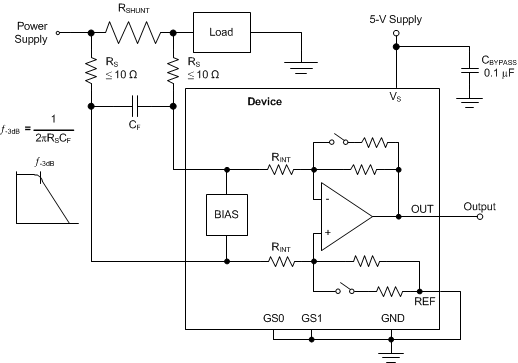 Figure 36. Input Filter
Care must be taken in the selection of the external filter component values because these components can affect device measurement accuracy. Placing external resistance in series with the input terminals creates an additional error so these resistors should be kept as low of a value as possible with a recommended maximum value of
10 Ω or less. Increasing the value of the input filter resistance beyond 10 Ω results in a smaller voltage signal present at the device input terminals than what is developed across the current-sense shunt resistor.
The internal bias network shown in Figure 36 creates a mismatch in the two input bias current paths when a differential voltage is applied between the input terminals. Under normal conditions, where no external resistance is added to the input paths, this mismatch of input bias currents has little effect on device operation or accuracy. However, when additional external resistance is added (such as for input filtering), the mismatch of input bias currents creates unequal voltage drops across these external components. The mismatched voltages result in a signal reaching the input terminals that is lower in value than the signal developed directly across the current-sensing resistor.
The amount of variance in the differential voltage present at the device input relative to the voltage developed at the shunt resistor is based both on the external series resistance value (RS) and the internal input resistors (RINT). The reduction of the shunt voltage reaching the device input terminals appears as a gain error when comparing the output voltage relative to the voltage across the shunt resistor. A factor can be calculated to determine the amount of gain error that is introduced by the addition of external series resistance.
The amount of error these external filter resistors introduce into the measurement can be calculated using the simplified gain error factor in Equation 1, where the gain error factor is calculated with Equation 2.
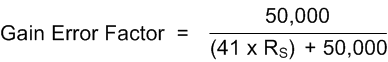
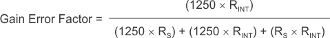
where
- RINT is the internal input impedance, and
- RS is the external series resistance.
For example, using the gain error factor (Equation 1), a 10-Ω series resistance results in a gain error factor of 0.992. The corresponding gain error is then calculated using Equation 3, resulting in a gain error of approximately 0.81% solely because of the external 10-Ω series resistors. Using 100-Ω filter resistors increases this gain error to approximately 7.58% from these resistors alone.

7.4.2 Shutting Down the Device
Although the device does not have a shutdown terminal, the low-power consumption allows for the device to be powered from the output of a logic gate or transistor switch that can turn on and turn off the voltage connected to the device power-supply terminal.
However, in current-shunt monitoring applications, there is also a concern for how much current is drained from the shunt circuit in shutdown conditions. Evaluating this current drain involves considering the device simplified schematic in shutdown mode, as shown in Figure 37.
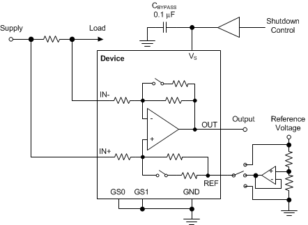 Figure 37. Shutting Down the Device
Note that there is typically a 525-kΩ impedance (from the combination of the 500-kΩ feedback and 25-kΩ input resistors) from each device input to the REF terminal. The amount of current flowing through these terminals depends on the respective configuration. For example, if the REF terminal is grounded, calculating the effect of the 525-kΩ impedance from the shunt to ground is straightforward. However, if the reference or op amp is powered while the device is shut down, the calculation is direct. Instead of assuming 525 kΩ to ground, assume 525 kΩ to the reference voltage. If the reference or op amp is also shut down, some knowledge of the reference or op amp output impedance under shutdown conditions is required. For instance, if the reference source behaves similar to an open circuit when un-powered, little or no current flows through the 525-kΩ path.
7.4.3 Using the Device with Common-Mode Transients Above 36 V
With a small amount of additional circuitry, the device can be used in circuits subject to transients higher than
36 V (such as automotive applications). Use only zener diodes or zener-type transient absorbers (sometimes referred to as transzorbs); any other type of transient absorber has an unacceptable time delay. Start by adding a pair of resistors, as shown in Figure 38, as a working impedance for the zener. Keeping these resistors as small as possible is preferable, most often around 10 Ω. This value limits the impact on accuracy with the addition of these external components, as described in the Input Filtering section. Larger values can be used if necessary with the result having an impact on gain error. Because this circuit limits only short-term transients, many applications are satisfied with a 10-Ω resistor along with conventional zener diodes of the lowest power rating available. This combination uses the least amount of board space. These diodes can be found in packages as small as SOT-523 or SOD-523.
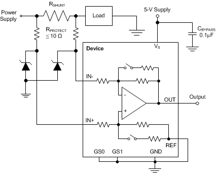 Figure 38. Device Transient Protection