ZHCSC53A February 2014 – March 2014 INA225
PRODUCTION DATA.
- 1 特性
- 2 应用范围
- 3 说明
- 4 修订历史记录
- 5 Terminal Configuration and Functions
- 6 Specifications
- 7 Detailed Description
- 8 Applications and Implementation
- 9 Power Supply Recommendations
- 10Layout
- 11器件和文档支持
- 12机械封装和可订购信息
5 Terminal Configuration and Functions
DGK Package
MSOP-8
(Top View)
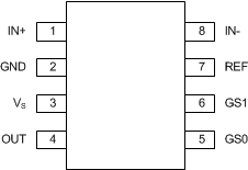
Terminal Functions
| TERMINAL | I/O | DESCRIPTION | |
|---|---|---|---|
| NAME | NO. | ||
| IN+ | 1 | Analog input | Connect to supply side of shunt resistor. |
| GND | 2 | Analog | Ground |
| VS | 3 | Analog | Power supply, 2.7 V to 36 V |
| OUT | 4 | Analog output | Output voltage |
| GS0 | 5 | Digital input | Gain select. Connect to VS or GND. Table 3 lists terminal settings and the corresponding gain value. |
| GS1 | 6 | Digital input | Gain select. Connect to VS or GND. Table 3 lists terminal settings and the corresponding gain value. |
| REF | 7 | Analog input | Reference voltage, 0 V to VS |
| IN– | 8 | Analog input | Connect to load side of shunt resistor. |