SBOS247C June 2002 – November 2015 INA217
PRODUCTION DATA.
- 1 Features
- 2 Applications
- 3 Description
- 4 Revision History
- 5 Pin Configuration and Functions
- 6 Specifications
- 7 Detailed Description
- 8 Application and Implementation
- 9 Power Supply Recommendations
- 10Layout
- 11Device and Documentation Support
- 12Mechanical, Packaging, and Orderable Information
6 Specifications
6.1 Absolute Maximum Ratings
over operating free-air temperature range (unless otherwise noted) (1)| MIN | MAX | UNIT | |||
|---|---|---|---|---|---|
| V+ to V– | Supply voltage | ±18 | V | ||
| Signal input terminals | Voltage(2) | (V–) – 0.5 | (V+) + 0.5 | V | |
| Current(2) | 10 | mA | |||
| Output short circuit(3) | Continuous | ||||
| Operating temperature | –55 | 125 | °C | ||
| Junction temperature | 300 | °C | |||
| Tstg | Storage temperature | –55 | 150 | °C | |
(1) Stresses beyond those listed under Absolute Maximum Ratings may cause permanent damage to the device. These are stress ratings only, which do not imply functional operation of the device at these or any other conditions beyond those indicated under Recommended Operating Conditions. Exposure to absolute-maximum-rated conditions for extended periods may affect device reliability.
(2) Input terminals are diode-clamped to the power-supply rails. Input signals that can swing more than 0.5 V beyond the supply rails should be current limited to 10 mA or less.
(3) Short-circuit to ground, one amplifier per package.
6.2 ESD Ratings
| VALUE | UNIT | |||
|---|---|---|---|---|
| V(ESD) | Electrostatic discharge | Human-body model (HBM), per ANSI/ESDA/JEDEC JS-001(1) | ±4000 | V |
| Charged-device model (CDM), per JEDEC specification JESD22-C101(2) | ±1000 | |||
(1) JEDEC document JEP155 states that 500-V HBM allows safe manufacturing with a standard ESD control process.
(2) JEDEC document JEP157 states that 250-V CDM allows safe manufacturing with a standard ESD control process.
6.3 Recommended Operating Conditions
over operating free-air temperature range (unless otherwise noted)| MIN | NOM | MAX | UNIT | ||
|---|---|---|---|---|---|
| V+ to V– | Supply voltage | ±4.5 | ±15 | ±18 | V |
| TA | Ambient Temperature | -40 | 25 | 85 | °C |
6.4 Thermal Information
| THERMAL METRIC(1) | INA217 | UNIT | ||
|---|---|---|---|---|
| DW (SOIC) | P (PDIP) | |||
| 16 PINS | 8 PINS | |||
| RθJA | Junction-to-ambient thermal resistance | 64.3 | 46.2 | °C/W |
| RθJC(top) | Junction-to-case (top) thermal resistance | 24.9 | 34.5 | °C/W |
| RθJB | Junction-to-board thermal resistance | 29.4 | 23.5 | °C/W |
| ψJT | Junction-to-top characterization parameter | 3.3 | 11.7 | °C/W |
| ψJB | Junction-to-board characterization parameter | 28.8 | 23.3 | °C/W |
| RθJC(bot) | Junction-to-case (bottom) thermal resistance | N/A | N/A | °C/W |
(1) For more information about traditional and new thermal metrics, see the Semiconductor and IC Package Thermal Metrics application report, SPRA953.
6.5 Electrical Characteristics: VS = ±15 V
TA = 25°C, RL = 2 kΩ, VS = ±15 V, unless otherwise noted.| PARAMETER | TEST CONDITIONS | TA = 25°C | UNIT | |||
|---|---|---|---|---|---|---|
| MIN | TYP | MAX | ||||
| GAIN EQUATION(1) | G = 1 + 10k/RG | |||||
| Range | 1 to 10000 | V/V | ||||
| Gain Error | G = 1 | ±0.1% | ±0.25% | |||
| G = 10 | ±0.2% | ±0.7% | ||||
| G = 100 | ±0.2% | |||||
| G = 1000 | ±0.5% | |||||
| GAIN TEMPERATURE DRIFT COEFFICIENT | ||||||
| G = 1 | TA = –40°C to 85°C | ±3 | ±10 | ppm/°C | ||
| G > 10 | TA = –40°C to 85°C | ±40 | ±100 | ppm/°C | ||
| Nonlinearity | G = 1 | ±0.0003 | % of FS | |||
| G = 100 | ±0.0006 | % of FS | ||||
| INPUT STAGE NOISE | ||||||
| Voltage Noise | fO = 1 kHz | RSOURCE = 0 Ω | 1.3 | nV/√Hz | ||
| fO = 100 Hz | 1.5 | nV/√Hz | ||||
| fO = 10 Hz | 3.5 | nV/√Hz | ||||
| Current Noise, | fO = 1 kHz | 0.8 | pA/√Hz | |||
| OUTPUT STAGE NOISE | ||||||
| Voltage Noise, | fO = 1 kHz | 90 | nV/√Hz | |||
| INPUT OFFSET VOLTAGE | ||||||
| Input Offset Voltage | VCM = VOUT = 0 V | 50 + 2000/G | 250 + 5000/G | µV | ||
| vs Temperature | TA = –40°C to 85°C | 1 + 20/G | µV/°C | |||
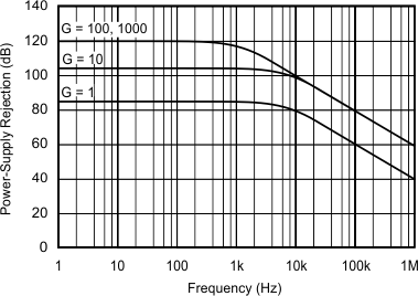
| vs Power Supply | VS = ±4.5 V to ±18 V | 1 + 50/G | 3 + 200/G | µV/V | ||
| INPUT VOLTAGE RANGE | ||||||
| Common-Mode Voltage Range | VIN+ – VIN– = 0V | (V+) – 4 | (V+) – 3 | V | ||
| VIN+ – VIN– = 0V | (V–) + 4 | (V–) + 3 | V | |||
| Common-Mode Rejection | G = 1 | VCM = ±11 V, RSRC = 0 Ω | 70 | 80 | dB | |
| G = 100 | 100 | 116 | dB | |||
| INPUT BIAS CURRENT | ||||||
| Initial Bias Current | 2 | 12 | µA | |||
| vs Temperature | TA = –40°C to 85°C | 10 | nA/°C | |||
| Initial Offset Current | 0.1 | 1 | µA | |||
| vs Temperature | TA = –40°C to 85°C | 0.5 | nA/°C | |||
| INPUT IMPEDANCE | ||||||
| Differential | 60 || 2 | MΩ || pF | ||||
| Common-Mode | 60 || 2 | MΩ || pF | ||||
| DYNAMIC RESPONSE | ||||||
| Bandwidth, Small Signal, –3d B | ||||||
| G = 1 | 3.4 | MHz | ||||
| G = 100 | 800 | kHz | ||||
| Slew Rate | 15 | V/µs | ||||
| THD+Noise, f = 1 kHz | G = 100 | 0.004% | ||||
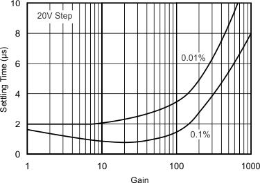
| Settling Time | 0.1% | G = 100, 10V Step | 2 | µs | ||
| 0.01% | G = 100, 10V Step | 3.5 | µs | |||
| Overload Recovery | 50% Overdrive | 1 | µs | |||
| OUTPUT | ||||||
| Voltage | RL to GND | (V+) – 2 (V–) + 2 |
(V+) – 1.8 (V–) + 1.8 |
V V |
||
| Load Capacitance Stability | 1000 | pF | ||||
| Short Circuit Current | Continuous-to-Common | ±60 | mA | |||
| POWER SUPPLY | ||||||
| Rated Voltage | ±15 | V | ||||
| Voltage Range | ±4.5 | ±18 | V | |||
| Current, Quiescent | IO = 0 mA | ±10 | ±12 | mA | ||
| TEMPERATURE RANGE | ||||||
| Specification | –40 | 85 | °C | |||
| Operating | –40 | 125 | °C | |||
(1) Gain accuracy is a function of external RG.
6.6 Typical Characteristics
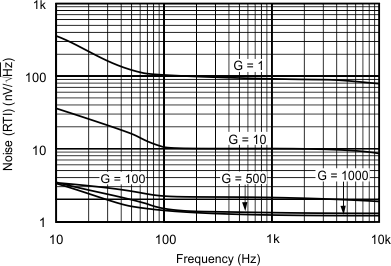
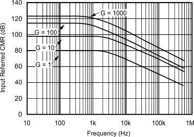
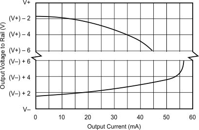
At TA = 25°C, VS = ±15 V, RL = 2 kΩ, unless otherwise noted.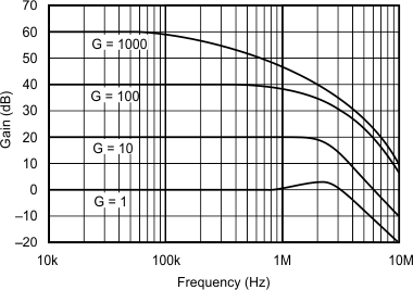
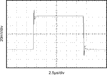
| G = 1 |
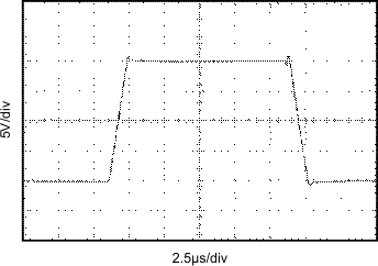
| G = 1 |
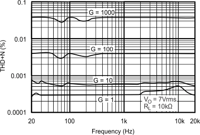
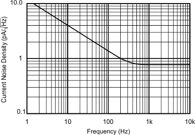
| G = 100 |
| G = 100 |