SBOS247C June 2002 – November 2015 INA217
PRODUCTION DATA.
- 1 Features
- 2 Applications
- 3 Description
- 4 Revision History
- 5 Pin Configuration and Functions
- 6 Specifications
- 7 Detailed Description
- 8 Application and Implementation
- 9 Power Supply Recommendations
- 10Layout
- 11Device and Documentation Support
- 12Mechanical, Packaging, and Orderable Information
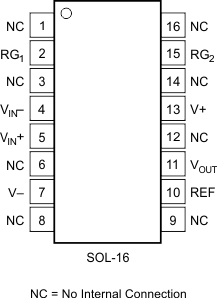
5 Pin Configuration and Functions
DW Package
16-Pin SOIC
Top View

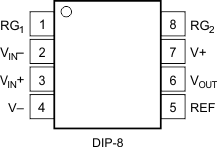
P Package
8-Pin PDIP
Top View

Pin Functions
| PIN | I/O | DESCRIPTION | |
|---|---|---|---|
| NAME | NO. | ||
| PDIP | |||
| NC | 1 | — | No internal connection |
| RG1 | 2 | I | Gain setting pin, for gains greater than one, connect an external resistor between pins 2 and 15 |
| NC | 3 | — | No internal connection |
| VIN– | 4 | I | Inverting input |
| VIN+ | 5 | I | Non-inverting input |
| NC | 6 | — | No internal connection |
| V– | 7 | I | negative power supply |
| NC | 8 | — | No internal connection |
| NC | 9 | — | No internal connection |
| REF | 10 | I | Reference input |
| VOUT | 11 | O | Output |
| NC | 12 | — | No internal connection |
| V+ | 13 | I | Positive power supply |
| NC | 14 | — | No internal connection |
| RG2 | 15 | I | Gain setting pin, for gains greater than one, connect an external resistor between pins 2 and 15 |
| NC | 16 | — | No internal connection |
| SOIC | |||
| RG1 | 1 | I | Gain setting pin, for gains greater than one, connect an external resistor between pins 1 and 8 |
| VIN– | 2 | I | Inverting input |
| VIN+ | 3 | I | Non-inverting input |
| V– | 4 | I | negative power supply |
| REF | 5 | I | Reference input |
| VOUT | 6 | O | Output |
| V+ | 7 | I | Positive power supply |
| RG2 | 8 | I | Gain setting pin, for gains greater than one, connect an external resistor between pins 2 and 15 |