ZHCSJE3C february 2019 – august 2021 INA191 , INA2191
PRODUCTION DATA
- 1
- 1 特性
- 2 应用
- 3 说明
- 4 Revision History
- 5 Pin Configuration and Functions
- 6 Specifications
- 7 Detailed Description
- 8 Application and Implementation
- 9 Power Supply Recommendations
- 10Layout
- 11Device and Documentation Support
- 12Mechanical, Packaging, and Orderable Information
5 Pin Configuration and Functions
 Figure 5-1 INA191 YFD Package6-Pin DSBGA
Top View
Figure 5-1 INA191 YFD Package6-Pin DSBGA
Top ViewTable 5-1 Pin Functions (INA191)
| PIN | TYPE | DESCRIPTION | |
|---|---|---|---|
| NAME | NO. | ||
| ENABLE | B3 | Digital input | Enable pin. When this pin is driven to VS, the device is on and functions as a current sense amplifier. When this pin is driven to GND, the device is off, the supply current is reduced, and the output is placed in a high-impedance state. This pin must be driven externally, or connected to VS if not used. |
| GND | B2 | Analog | Ground. |
| IN+ | A1 | Analog input | Current-shunt monitor positive input. For high-side applications, connect this pin to the bus voltage side of the sense resistor. For low-side applications, connect this pin to the load side of the sense resistor. |
| IN– | B1 | Analog input | Current-shunt monitor negative input. For high-side applications, connect this pin to the load side of the sense resistor. For low-side applications, connect this pin to the ground side of the sense resistor. |
| OUT | A3 | Analog output | This pin provides an analog voltage output that is the amplified voltage difference from the IN+ to the IN– pins. |
| VS | A2 | Analog | Power supply, 1.7 V to 5.5 V. |
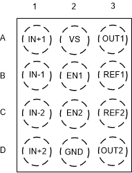
 Figure 5-2 INA2191 YBJ Package12-Pin DSBGATop View
Table 5-2 Pin Functions
(INA2191)
| PIN | TYPE | DESCRIPTION | |
|---|---|---|---|
| NAME | NO. | ||
| ENABLE1 | B2 | Digital input | Enable pin for output 1. When this pin is driven to VS, channel 1 is on and functions as a current sense amplifier. When both enable pins are driven to GND, the device is off and the supply current is reduced. This pin must be driven externally, or connected to VS if not used. |
| ENABLE2 | C2 | Digital input | Enable pin for output 2. When this pin is driven to VS, channel 2 is on and functions as a current sense amplifier. When both enable pins are driven to GND, the device is off and the supply current is reduced. This pin must be driven externally, or connected to VS if not used. |
| GND | D2 | Analog | Ground. |
| IN+1 | A1 | Analog input | Current-shunt monitor positive input for channel 1. For high-side applications, connect this pin to the bus voltage side of the sense resistor. For low-side applications, connect this pin to the load side of the sense resistor. |
| IN+2 | D1 | Analog input | Current-shunt monitor positive input for channel 2. For high-side applications, connect this pin to the bus voltage side of the sense resistor. For low-side applications, connect this pin to the load side of the sense resistor. |
| IN–1 | B1 | Analog input | Current-shunt monitor negative input for channel 1. For high-side applications, connect this pin to the load side of the sense resistor. For low-side applications, connect this pin to the ground side of the sense resistor. |
| IN–2 | C1 | Analog input | Current-shunt monitor negative input for channel 2. For high-side applications, connect this pin to the load side of the sense resistor. For low-side applications, connect this pin to the ground side of the sense resistor. |
| OUT1 | A3 | Analog output | This pin provides an analog voltage output that is the amplified voltage difference from the IN+1 to the IN–1 pins, and is offset by the voltage applied to the REF1 pin. |
| OUT2 | D3 | Analog output | This pin provides an analog voltage output that is the amplified voltage difference from the IN+2 to the IN–2 pins, and is offset by the voltage applied to the REF2 pin. |
| REF1 | B3 | Analog input | Reference input for channel 1. Enables bidirectional current sensing for channel 1 with an externally applied voltage. |
| REF2 | C3 | Analog input | Reference input for channel 2. Enables bidirectional current sensing for channel 2 with an externally applied voltage. |
| VS | A2 | Analog | Power supply, 1.7 V to 5.5 V. |