ZHCSJE3C february 2019 – august 2021 INA191 , INA2191
PRODUCTION DATA
- 1
- 1 特性
- 2 应用
- 3 说明
- 4 Revision History
- 5 Pin Configuration and Functions
- 6 Specifications
- 7 Detailed Description
- 8 Application and Implementation
- 9 Power Supply Recommendations
- 10Layout
- 11Device and Documentation Support
- 12Mechanical, Packaging, and Orderable Information
8.1.3 Signal Conditioning
When performing accurate current measurements in noisy environments, the current-sensing signal is often filtered. The INAx191 features low input bias currents. Therefore, it is possible to add a differential mode filter to the input without sacrificing the current-sense accuracy. Filtering at the input is advantageous because this action attenuates differential noise before the signal is amplified. Figure 8-2 provides an example of how to use a filter on the input pins of the device.
 Figure 8-2 Filter at the Input Pins
The differential input impedance (RDIFF) shown in Figure 8-2 limits the maximum value for RF. The value of RDIFF is a function of the device temperature and gain option, as shown in Figure 8-3.
 Figure 8-3 Differential Input Impedance vs. Temperature
As the voltage drop across the sense resistor (VSENSE) increases, the amount of voltage dropped across the input filter resistors (RF) also increases. The increased voltage drop results in additional gain error. The error caused by these resistors is calculated by the resistor divider equation shown in Equation 5.
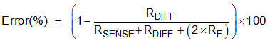
where:
- RSENSE is the current sense resistor, as defined in Equation 2.
- RDIFF is the differential input impedance.
- RF is the added value of the series filter resistance.
The input stage of the INAx191 uses a capacitive feedback amplifier topology in order to achieve high DC precision. As a result, periodic high-frequency shunt voltage (or current) transients of significant amplitude (10 mV or greater) and duration (hundreds of nanoseconds or greater) may be amplified by the INAx191, even though the transients are greater than the device bandwidth. Use a differential input filter in these applications to minimize disturbances at the INAx191 output.
The high input impedance and low bias current of the INAx191 provides flexibility in the input filter design without impacting the accuracy of current measurement. For example, set RF = 100 Ω and CF = 22 nF to achieve a low-pass filter corner frequency of 36.2 kHz. These filter values significantly attenuate most unwanted high-frequency signals at the input without severely impacting the current-sensing bandwidth or precision. If a lower corner frequency is desired, increase the value of CF.
Filtering at the input reduces differential noise across the sense resistor. If high-frequency, common-mode noise is a concern, add an RC filter from the OUT pin to ground. The RC filter helps filter out both differential and common mode noise, as well as internally generated noise from the device. The value for the resistance of the RC filter is limited by the impedance of the output load. Any current drawn by the load manifests as an external voltage drop from the INAx191 OUT pin to the load input. To select the optimal values for the output filter when driving SAR ADCs or other dynamic loads, use Figure 6-41 and see the Closed-Loop Analysis of Load-Induced Amplifier Stability Issues Using ZOUT Application Report