ZHCSNB1 February   2021 INA183

PRODUCTION DATA  

  1. 特性
  2. 应用
  3. 说明
  4. Revision History
  5. Device Comparison
  6. Pin Configuration and Functions
  7. Specifications
    1. 7.1 Absolute Maximum Ratings
    2. 7.2 ESD Ratings
    3. 7.3 Recommended Operating Conditions
    4. 7.4 Thermal Information
    5. 7.5 Electrical Characteristics
    6. 7.6 Typical Characteristics
  8. Detailed Description
    1. 8.1 Overview
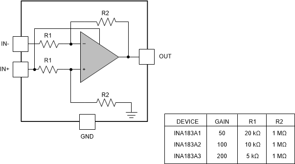
    2. 8.2 Functional Block Diagram
    3. 8.3 Feature Description
      1. 8.3.1 Single-Supply Operation from IN+
      2. 8.3.2 Low Gain Error and Offset Voltage
      3. 8.3.3 Low Drift Architecture
    4. 8.4 Device Functional Modes
      1. 8.4.1 Normal Operation
      2. 8.4.2 Unidirectional, High-Side Operation
      3. 8.4.3 Input Differential Overload
  9. Application and Implementation
    1. 9.1 Application Information
      1. 9.1.1 RSENSE and Device Gain Selection
    2. 9.2 Typical Application
      1. 9.2.1 Design Requirements
      2. 9.2.2 Detailed Design Procedure
      3. 9.2.3 Application Curve
  10. 10Power Supply Recommendations
  11. 11Layout
    1. 11.1 Layout Guidelines
    2. 11.2 Layout Example
  12. 12Device and Documentation Support
    1. 12.1 Documentation Support
      1. 12.1.1 Related Documentation
    2. 12.2 接收文档更新通知
    3. 12.3 支持资源
    4. 12.4 Trademarks
    5. 12.5 静电放电警告
    6. 12.6 术语表
  13. 13Mechanical, Packaging, and Orderable Information

封装选项

机械数据 (封装 | 引脚)
散热焊盘机械数据 (封装 | 引脚)
订购信息

Functional Block Diagram

The simplified functional diagram below shows the device power is provided by the voltage on the IN+ pin. This diagram also shows the nominal values for the internal gain set resistors. The nominal value of these resistors can vary by 20% or more; however, the matching between these resistors is tightly controlled. The matching of these internal resistors results in a precise fixed gain that varies very little over temperature.

GUID-20210114-CA0I-N13M-Z6FX-GJSPFBXZDPC6-low.gif