ZHCSTC7A September 2000 – January 2024 INA114
PRODUCTION DATA
- 1
- 1 特性
- 2 应用
- 3 说明
- 4 Pin Configuration and Functions
- 5 Specifications
- 6 Application and Implementation
- 7 Typical Applications
- 8 Device and Documentation Support
- 9 Revision History
- 10Mechanical, Packaging, and Orderable Information
封装选项
请参考 PDF 数据表获取器件具体的封装图。
机械数据 (封装 | 引脚)
- P|8
- DW|16
散热焊盘机械数据 (封装 | 引脚)
订购信息
6.1.3 Offset Trimming
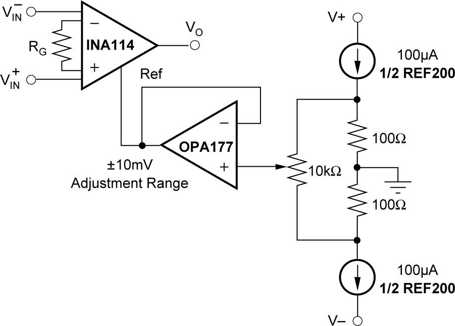
The INA114 is laser trimmed for very low offset voltage and drift. Most applications require no external offset adjustment. Figure 6-2 shows an optional circuit for trimming the output offset voltage. The voltage applied to the Ref pin is summed at the output. Maintain low impedance at this node to maintain good common-mode rejection by buffering trim voltage with an op amp as shown.
 Figure 6-2 Optional Trimming of Output Offset Voltage.