ZHCSCW0A October 2014 – November 2014 HDC1008
PRODUCTION DATA.
- 1 特性
- 2 应用
- 3 说明
- 4 典型应用
- 5 修订历史记录
- 6 Pin Configuration and Functions
- 7 Specifications
- 8 Detailed Description
- 9 Application and Implementation
- 10Power Supply Recommendations
- 11Layout
- 12器件和文档支持
- 13机械封装和可订购信息
7 Specifications
7.1 Absolute Maximum Ratings(1)
| MIN | MAX | UNIT | ||
|---|---|---|---|---|
| Input Voltage | VDD | -0.3 | 6 | V |
| SCL | -0.3 | 6 | ||
| SDA | -0.3 | 6 | ||
| DRDYn | -0.3 | 6 | ||
| ADR0 | -0.3 | VDD+0.3 | ||
| ADR1 | -0.3 | VDD+0.3 |
(1) Stresses beyond those listed under Absolute Maximum Ratings may cause permanent damage to the device. These are stress ratings only, which do not imply functional operation of the device at these or any other conditions beyond those indicated under Recommended Operating Conditions. Exposure to absolute-maximum-rated conditions for extended periods may affect device reliability.
7.2 Handling Ratings
| MIN | MAX | UNIT | |||
|---|---|---|---|---|---|
| TSTG | Storage Temperature(1) | -65 | 150 | °C | |
| V(ESD) | Electrostatic discharge | Human body model (HBM), per ANSI/ESDA/JEDEC JS-001, all pins (2) | -1000 | 1000 | V |
| Charged device model (CDM), per JEDEC specification –500 500 JESD22-C101, all pins (3) | -250 | 250 | |||
(1) For long term storage, it is recommended to stay within 10%RH-80%RH and +5°C to 60°C. Storage beyond this range may result in a temporary RH offset shift.
(2) JEDEC document JEP155 states that 500-V HBM allows safe manufacturing with a standard ESD control process.
(3) JEDEC document JEP157 states that 250-V CDM allows safe manufacturing with a standard ESD control process.
7.3 Recommended Operating Conditions
over operating range (unless otherwise noted)| MIN | NOM | MAX | UNIT | ||
|---|---|---|---|---|---|
| VDD | Supply Voltage | 2.7 | 3 | 5.5 | V |
| TA | Ambient Operating Temperature | -40 | 125 | °C | |
7.4 Thermal Information
| THERMAL METRIC(1) | HDC1008 | UNIT | |
|---|---|---|---|
| DSBGA | |||
| 8 PINS | |||
| RθJA | Junction-to-Ambient Thermal Resistance | 98.0 | °C/W |
(1) For more information about traditional and new thermal metrics, see the: IC Package Thermal Metrics application report, SPRA953.
7.5 Electrical Characteristics
The electrical ratings specified in this section apply to all specifications in this document, unless otherwise noted. TA = 30°C, VDD = 3V.| PARAMETER | TEST CONDITION | MIN | TYP | MAX | UNIT | |
|---|---|---|---|---|---|---|
| POWER CONSUMPTION | ||||||
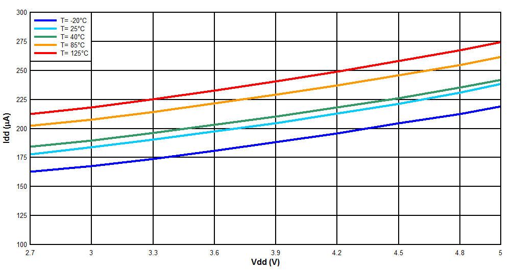
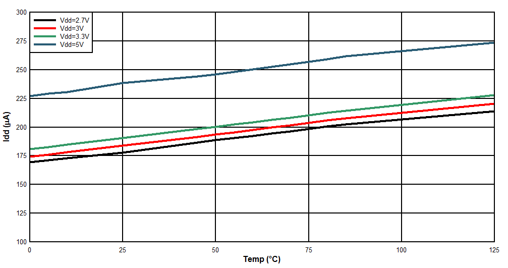
| IDD | Supply Current | RH measurement, bit 12 of 0x02 register = 0(6) | 180 | 220 | µA | |
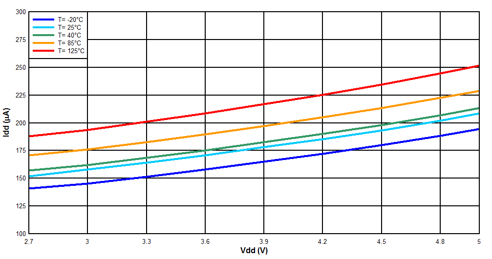
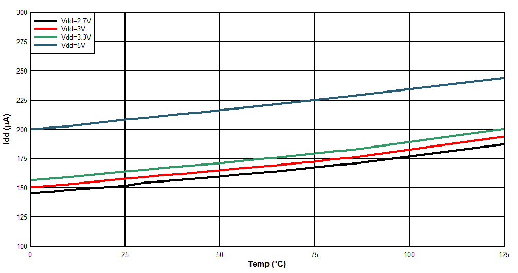
| Temperature measurement, bit 12 of 0x02 register = 0(6) | 155 | 185 | µA | |||
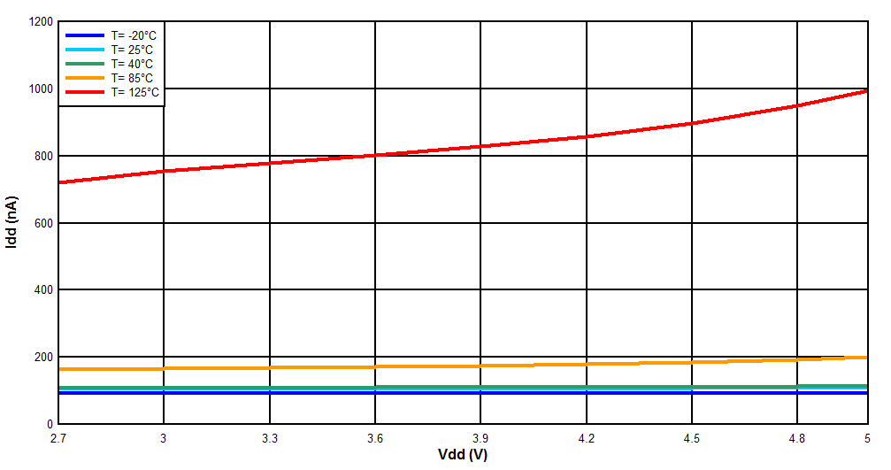
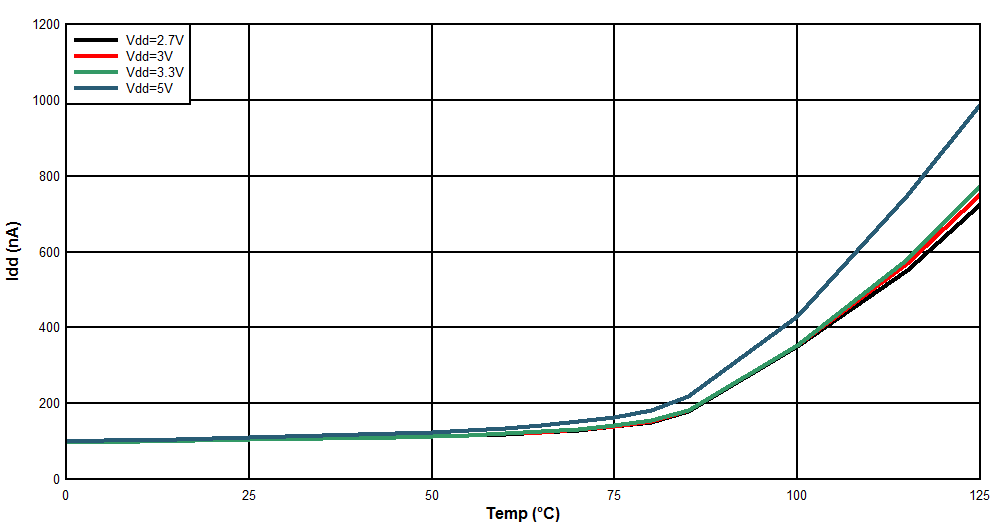
| Sleep Mode | 110 | 200 | nA | |||
| Average @ 1 measurement/second, RH (11 bit), bit 12 of 0x02 register = 0(6)(7) | 730 | nA | ||||
| Average @ 1 measurement/second, Temp (11 bit), bit 12 of 0x02 register = 0(6)(7) | 580 | nA | ||||
| Average @ 1 measurement/second, RH (11bit) +temperature (11 bit), bit 12 of 0x02 register = 1(6)(7) | 1.2 | µA | ||||
| Startup (average on Start-up time) | 300 | µA | ||||
| IHEAT | Heater Current(1) | Peak current | 7.6 | mA | ||
| Average @ 1 measurement/second, RH (11bit) +temperature (11 bit), bit 12 of 0x02 register = 1(6)(7) | 57 | µA | ||||
| RELATIVE HUMIDITY SENSOR | ||||||
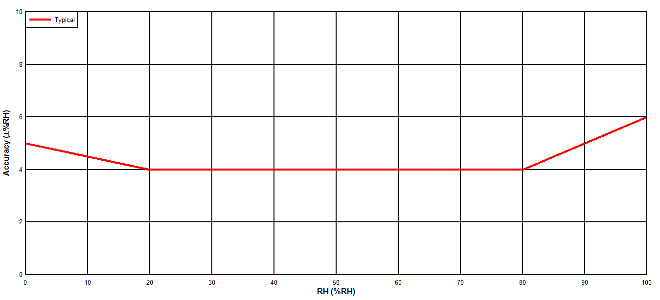
| RHACC | Accuracy | ±4 | %RH | |||
| RHREP | Repeatability(1) | 0%RH | ±0.1 | %RH | ||
| RHHYS | Hysteresis (3) | ±1 | %RH | |||
| RHRT | Response Time(5) | t 63% (4) | 15 | s | ||
| RHCT | Conversion Time(1) | 8 bit resolution | 2.50 | ms | ||
| 11 bit resolution | 3.85 | ms | ||||
| 14 bit resolution | 6.50 | ms | ||||
| RHHOR | Operating Range(2) | Non-condensing | 0 | 100 | %RH | |
| RHLTD | Long Term Drift | ±0.5 | %RH/yr | |||
| TEMPERATURE SENSOR | ||||||
| TEMPACC | Accuracy(1) | 5°C < TA< 60°C | ±0.2 | ±0.4 | °C | |
| TEMPREP | Repeatability(1) | ±0.1 | °C | |||
| TEMPCT | Conversion Time(1) | 11 bit accuracy | 3.65 | ms | ||
| 14 bit accuracy | 6.35 | ms | ||||
| TEMPOR | Operating Range | -40 | 125 | °C | ||
(1) This parameter is specified by design and/or characterization and it is not tested in production.
(2) Recommended humidity operating range is 10% to 80% RH. Prolonged operation outside these ranges may result in a measurement shift. The measurement shift will decrease after operating the sensor in the recommended operating range.
(3) The hysteresis value is the difference of measured values of a given sensor at a certain measuring point accruing from a dry environment to a humid environment after a dwell time.
(4) Time for the RH output to change by 63% of the total RH change after a step change in environmental humidity.
(5) Actual response times will vary dependent on system thermal mass and air-flow.
(6) I2C read/write communication and pull-up resistors current through SCL, SDA and DRDYn not included.
(7) Average current consumption while conversion is in progress.
7.6 I2C Interface Electrical Characteristics
At TA=30°C, VDD=3V (unless otherwise noted)| PARAMETER | TEST CONDITION | MIN | TYP | MAX | UNIT | |
|---|---|---|---|---|---|---|
| I2C INTERFACE VOLTAGE LEVEL | ||||||
| VIH | Input High Voltage | 0.7xVDD | V | |||
| VIL | Input Low Voltage | 0.3xVDD | V | |||
| VOL | Output Low Voltage | Sink current 3mA | 0.4 | V | ||
| HYS | Hysteresis (1) | 0.1xVDD | V | |||
| CIN | Input Capacitance on all digital pins | 0.5 | pF | |||
(1) This parameter is specified by design and/or characterization and it is not tested in production.
7.7 I2C Interface Timing Requirements
| PARAMETER | TEST CONDITION | MIN | TYP | MAX | UNIT | |
|---|---|---|---|---|---|---|
| I2C INTERFACE VOLTAGE LEVEL | ||||||
| fSCL | Clock Frequency | 10 | 400 | kHz | ||
| tLOW | Clock Low Time | 1.3 | µs | |||
| tHIGH | Clock High Time | 0.6 | µs | |||
| tSP | Pulse width of spikes that must be suppressed by the input filter (1) | 50 | ns | |||
| tSTART | Device Start-up time | From VDD ≥ 2.7 V to ready for a conversion(1)(2) | 10 | 15 | ms | |
(1) This parameter is specified by design and/or characterization and it is not tested in production.
(2) Within this interval it is not possible to communicate to the device.
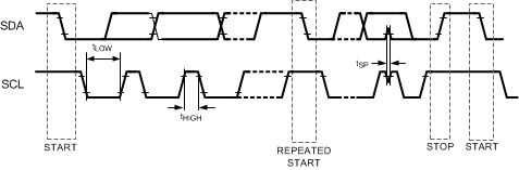 Figure 1. I2C Timing
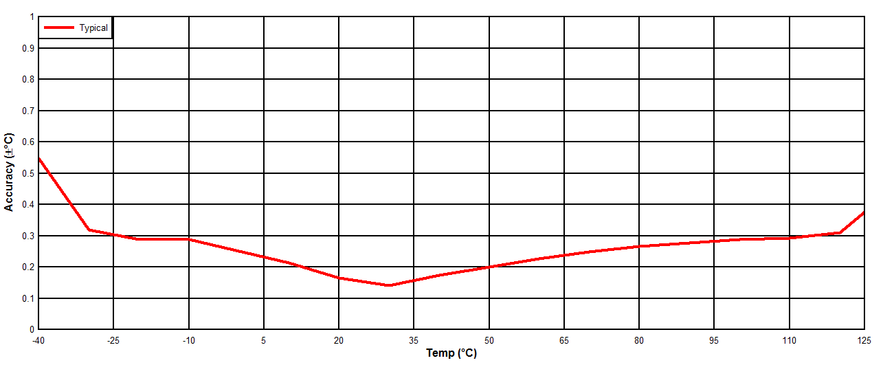
7.8 Typical Characteristics
Unless otherwise noted, TA = 30°C, VDD = 3V.