ZHCSCW0A October 2014 – November 2014 HDC1008
PRODUCTION DATA.
- 1 特性
- 2 应用
- 3 说明
- 4 典型应用
- 5 修订历史记录
- 6 Pin Configuration and Functions
- 7 Specifications
- 8 Detailed Description
- 9 Application and Implementation
- 10Power Supply Recommendations
- 11Layout
- 12器件和文档支持
- 13机械封装和可订购信息
6 Pin Configuration and Functions
WLCSP (DSBGA)
8 Pin
Top View
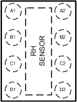
Pin Functions
| PIN | I/O TYPE(1) | DESCRIPTION | |
|---|---|---|---|
| NAME | NO. | ||
| SCL | A1 | I | Serial clock line for I2C, open-drain; requires a pull-up resistor to VDD |
| VDD | B1 | P | Supply Voltage |
| ADR0 | C1 | I | Address select pin – hardwired to GND or VDD |
| ADR1 | D1 | I | Address select pin – hardwired to GND or VDD |
| SDA | A2 | I/O | Serial data line for I2C, open-drain; requires a pull-up resistor to VDD |
| GND | B2 | G | Ground |
| DNC | C2 | - | Do Not Connect or connect to GND |
| DRDYn | D2 | O | Data ready, active low, open-drain; requires a pull-up resistor to VDD. If not used tie to GND or no connect. |
(1) P=Power, G=Ground, I=Input, O=Output