ZHCSDQ7 May 2015 HD3SS3212
PRODUCTION DATA.
- 1 特性
- 2 应用
- 3 说明
- 4 简化电路原理图
- 5 修订历史记录
- 6 Device Comparison Table
- 7 Pin Configuration and Functions
- 8 Specifications
- 9 Parameter Measurement Information
- 10Detailed Description
- 11Application and Implementation
- 12Power Supply Recommendations
- 13Layout
- 14器件和文档支持
- 15机械、封装和可订购信息
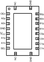
7 Pin Configuration and Functions
RKS Package
20-Pin VQFN
Top View

Pin Functions
| PIN | TYPE(1) | DESCRIPTION | |
|---|---|---|---|
| NAME | NO. | ||
| VCC | 6 | P | 3.3-V power |
| OEn | 2 | I | Active-low chip enable L: Normal operation H: Shutdown |
| A0p | 3 | I/O | Port A, channel 0, high-speed positive signal |
| A0n | 4 | I/O | Port A, channel 0, high-speed negative signal |
| GND | 5, 11, 20 | G | Ground |
| A1p | 7 | I/O | Port A, channel 1, high-speed positive signal |
| A1n | 8 | I/O | Port A, channel 1, high-speed negative signal |
| SEL | 9 | I | Port select pin. Internally tied to GND via 100-kΩ resistor. L: Port A to Port B H: Port A to Port C |
| C1n | 12 | I/O | Port C, channel 1, high-speed negative signal (connector side) |
| C1p | 13 | I/O | Port C, channel 1, high-speed positive signal (connector side) |
| C0n | 14 | I/O | Port C, channel 0, high-speed negative signal (connector side) |
| C0p | 15 | I/O | Port C, channel 0, high-speed positive signal (connector side) |
| B1n | 16 | I/O | Port B, channel 1, high-speed negative signal (connector side) |
| B1p | 17 | I/O | Port B, channel 1, high-speed positive signal (connector side) |
| B0n | 18 | I/O | Port B, channel 0, high-speed negative signal (connector side) |
| B0p | 19 | I/O | Port B, channel 0, high-speed positive signal (connector side) |
| NC | 1, 10 | NC | These are no connect pins but can be tied to VCC or GND |
(1) The high-speed data ports incorporate 20-kΩ pulldown resistors that are switched in when a port is not selected and switched out when the port is selected.