ZHCSR66C November   2022  – December 2022 ESD751 , ESD761

PRODUCTION DATA  

  1. 特性
  2. 应用
  3. 说明
  4. Revision History
  5. Pin Configuration and Functions
  6. Specifications
    1. 6.1 Absolute Maximum Ratings
    2. 6.2 ESD Ratings—JEDEC Specification
    3. 6.3 ESD Ratings—IEC Specification
    4. 6.4 Recommended Operating Conditions
    5. 6.5 Thermal Information
    6. 6.6 Electrical Characteristics
    7. 6.7 Typical Characteristics – ESD751
    8. 6.8 Typical Characteristics - ESD761
  7. Detailed Description
    1. 7.1 Overview
    2. 7.2 Functional Block Diagram
    3. 7.3 Feature Description
      1. 7.3.1 IEC 61000-4-5 Surge Protection
      2. 7.3.2 I/O Capacitance
    4. 7.4 Device Functional Modes
  8. Application and Implementation
    1. 8.1 Application Information
    2. 8.2 Typical Application
      1. 8.2.1 Design Requirements
      2. 8.2.2 Detailed Design Procedure
        1. 8.2.2.1 Application Curves
  9. Power Supply Recommendations
  10. 10Layout
    1. 10.1 Layout Guidelines
    2. 10.2 Layout Example
  11. 11Device and Documentation Support
    1. 11.1 Documentation Support
      1. 11.1.1 Related Documentation
    2. 11.2 接收文档更新通知
    3. 11.3 支持资源
    4. 11.4 Trademarks
    5. 11.5 Electrostatic Discharge Caution
    6. 11.6 术语表
  12. 12Mechanical, Packaging, and Orderable Information

封装选项

机械数据 (封装 | 引脚)
散热焊盘机械数据 (封装 | 引脚)
订购信息

Pin Configuration and Functions

GUID-624C0594-DB0C-443C-8F51-4851A0461A50-low.gifFigure 5-1 DPY Package, 2-Pin X1SON (Top View)
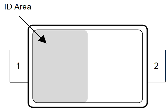
GUID-75C2A519-B43A-4D72-935D-5D4BC6D619AB-low.pngFigure 5-2 DYA Package, 2-Pin SOD523 (Top View)
Table 5-1 Pin Functions
PINTYPE(1)DESCRIPTION
NAMENO.
IO1I/OESD protected IO
GND2

G

Connect to ground.
I = Input, O = Output, I/O = Input or Output, G = Ground, P = Power.