ZHCSIV4 September   2018 DSLVDS1048

PRODUCTION DATA.  

  1. 特性
  2. 应用
  3. 说明
    1.     Device Images
      1. 3.1 703A I2C
  4. 修订历史记录
  5. Pin Configuration and Functions
    1.     Pin Functions
  6. Specifications
    1. 6.1 Absolute Maximum Ratings
    2. 6.2 ESD Ratings
    3. 6.3 Recommended Operating Conditions
    4. 6.4 Thermal Information
    5. 6.5 Electrical Characteristics
    6. 6.6 Switching Characteristics
    7. 6.7 Typical Characteristics
  7. Parameter Measurement Information
  8. Detailed Description
    1. 8.1 Overview
    2. 8.2 Functional Block Diagram
    3. 8.3 Feature Description
      1. 8.3.1 Fail-Safe Feature
    4. 8.4 Device Functional Modes
  9. Application and Implementation
    1. 9.1 Application Information
    2. 9.2 Typical Application
      1. 9.2.1 Design Requirements
      2. 9.2.2 Detailed Design Procedure
        1. 9.2.2.1 Probing LVDS Transmission Lines
        2. 9.2.2.2 Threshold
      3. 9.2.3 Application Curve
  10. 10Power Supply Recommendations
  11. 11Layout
    1. 11.1 Layout Guidelines
      1. 11.1.1 Power Decoupling Recommendations
      2. 11.1.2 Differential Traces
      3. 11.1.3 Termination
    2. 11.2 Layout Example
  12. 12器件和文档支持
    1. 12.1 接收文档更新通知
    2. 12.2 社区资源
    3. 12.3 商标
    4. 12.4 静电放电警告
    5. 12.5 术语表
  13. 13机械、封装和可订购信息

封装选项

机械数据 (封装 | 引脚)
散热焊盘机械数据 (封装 | 引脚)
订购信息

Pin Configuration and Functions

PW Package
16-Pin TSSOP
Top View
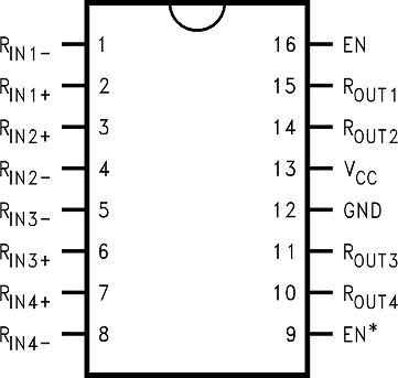
DSLVDS1048 10088801.png

Pin Functions

PIN I/O DESCRIPTION
NAME NO.
EN 16 I Receiver enable pin: When EN is low, the receiver is disabled. When EN is high and EN* is low or open, the receiver is enabled. If both EN and EN* are open circuit, then the receiver is disabled.
EN* 9 I Receiver enable pin: When EN* is high, the receiver is disabled. When EN* is low or open and EN is high, the receiver is enabled. If both EN and EN* are open circuit, then the receiver is disabled.
GND 12 Ground pin
RIN+ 2, 3, 6, 7 I Noninverting receiver input pin
RIN− 1, 4, 5, 8 I Inverting receiver input pin
ROUT 10, 11, 14, 15 O Receiver output pin
VCC 13 Power supply pin, +3.3V ± 0.3V