SNLS055J November 1999 – May 2016 DS90CF366 , DS90CF386
PRODUCTION DATA.
- 1 Features
- 2 Applications
- 3 Description
- 4 Revision History
- 5 Pin Configuration and Functions
- 6 Specifications
- 7 Detailed Description
- 8 Application and Implementation
- 9 Power Supply Recommendations
- 10Layout
- 11Device and Documentation Support
- 12Mechanical, Packaging, and Orderable Information
8 Application and Implementation
NOTE
Information in the following applications sections is not part of the TI component specification, and TI does not warrant its accuracy or completeness. TI’s customers are responsible for determining suitability of components for their purposes. Customers should validate and test their design implementation to confirm system functionality.
8.1 Application Information
The DS90F386 and DS90CF366 are designed for a wide variety of data transmission applications. The use of serialized LVDS data lines in these applications allows for efficient signal transmission over a narrow bus width, thereby reducing cost, power, and space.
8.2 Typical Applications
Figure 21 and Figure 22 show typical applications of the DS90CF386 and DS90CF366 for displays when used as an OpenLDI-to-RGB bridge.
 Figure 21. Typical DS90CF386 Application Block Diagram
 Figure 22. Typical DS90CF366 Application Block Diagram
8.2.1 Design Requirements
For this design example, follow the requirements in Table 1.
Table 1. Design Parameters
8.2.2 Detailed Design Procedure
To design with the DS90CF386 or DS90CF366, determine the following:
- Cable Interface
- Bit Resolution and Operating Frequency
- Bit Mapping from Receiver to Endpoint Panel Display
- RSKM Interoperability with Transmitter Pulse Position Margin
8.2.2.1 Cables
A cable interface between the transmitter and receiver needs to support the differential LVDS pairs. The DS90CF366 requires four pairs of signal wires and the DS90CF386 requires five pairs of signal wires. The ideal cable interface has a constant 100-Ω differential impedance throughout the path. It is also recommended that cable skew remain below 120 ps (assuming 85 MHz clock rate) to maintain a sufficient data sampling window at the receiver.
Depending upon the application and data rate, the interconnecting media between Tx and Rx may vary. For example, for lower data rate (clock rate) and shorter cable lengths (< 2m), the media electrical performance is less critical. For higher speed or long distance applications, the media's performance becomes more critical. Certain cable constructions provide tighter skew (matched electrical length between the conductors and pairs). For example, twin-coax cables have been demonstrated at distances as long as five meters and with the maximum data transfer of 2.38 Gbps (DS90CF366) and 1.785 Gbps (DS90CF386).
8.2.2.2 Bit Resolution and Operating Frequency Compatibility
The bit resolution of the endpoint panel display reveals whether there are enough bits available in the DS90CF386 or DS90CF366 to output the required data per pixel. The DS90CF386 has 28 parallel LVCMOS outputs and can therefore provide a bit resolution up to 24 bpp (bits per pixel). In each clock cycle, the remaining bits are the three control signals (HSync, VSync, DE) and one spare bit. The DS90CF366 has 21 parallel LVCMOS outputs and can therefore provide a bit resolution up to 18 bpp (bits per pixel). In each clock cycle, the remaining bits are the three control signals (HSync, VSync, DE).
The number of pixels per frame and the refresh rate of the endpoint panel display indicate the required operating frequency of the deserializer clock. To determine the required clock frequency, refer to Equation 1.
where
- H_Active = Active Display Horizontal Lines
- H_Blank = Blanking Period Horizontal Lines
- V_Active = Active Display Vertical Lines
- V_Blank = Blanking Period Vertical Lines
- f_Vertical = Refresh Rate (in Hz)
- f_Clk = Operating Frequency of LVDS clock
In each frame, there is a blanking period associated with horizontal rows and vertical columns that are not actively displayed on the panel. These blanking period pixels must be included to determine the required clock frequency. Consider the following example to determine the required LVDS clock frequency:
- H_Active = 640
- H_Blank = 40
- V_Active = 480
- V_Blank = 41
- f_Vertical = 59.95 Hz
Thus, the required operating frequency is determined with Equation 2.
Since the operating frequency for the PLL in the DS90CF386 and DS90CF366 ranges from 20 to 85 MHz, the DS90CF386 and DS90CF366 can support a panel display with the aforementioned requirements.
If the specific blanking interval is unknown, the number of pixels in the blanking interval can be approximated to 20% of the active pixels. Equation 3 can be used as a conservative approximation for the operating LVDS clock frequency:
Using this approximation, the operating frequency for the example in this section is estimated with Equation 4.
8.2.2.3 Data Mapping between Receiver and Endpoint Panel Display
Ensure that the LVCMOS outputs are mapped to align with the endpoint display RGB mapping requirements following the deserializer. See the following for two popular mapping topologies for 8-bit RGB data.
- LSBs are mapped to RxIN3±.
- MSBs are mapped to RxIN3±.
Table 2 and Table 3 depict how these two popular topologies can be mapped to the DS90CF386 outputs.
Table 2. 8-Bit Color Mapping with LSBs on RxIN3±
| LVDS INPUT CHANNEL | LVDS BIT STREAM POSITION | LVCMOS OUTPUT CHANNEL | COLOR MAPPING | COMMENTS |
|---|---|---|---|---|
| RxIN0 | TxIN0 | RxOUT0 | R2 | |
| TxIN1 | RxOUT1 | R3 | ||
| TxIN2 | RxOUT2 | R4 | ||
| TxIN3 | RxOUT3 | R5 | ||
| TxIN4 | RxOUT4 | R6 | ||
| TxIN6 | RxOUT6 | R7 | MSB | |
| RxIN1 | TxIN7 | RxOUT7 | G2 | |
| TxIN8 | RxOUT8 | G3 | ||
| TxIN9 | RxOUT9 | G4 | ||
| TxIN12 | RxOUT12 | G5 | ||
| TxIN13 | RxOUT13 | G6 | ||
| TxIN14 | RxOUT14 | G7 | MSB | |
| TxIN15 | RxOUT15 | B2 | ||
| TxIN18 | RxOUT18 | B3 | ||
| RxIN2 | TxIN19 | RxOUT19 | B4 | |
| TxIN20 | RxOUT20 | B5 | ||
| TxIN21 | RxOUT21 | B6 | ||
| TxIN22 | RxOUT22 | B7 | MSB | |
| TxIN24 | RxOUT24 | HSYNC | Horizontal sync | |
| TxIN25 | RxOUT25 | VSYNC | Vertical sync | |
| TxIN26 | RxOUT26 | DE | Data enable | |
| RxIN3 | TxIN27 | RxOUT27 | R0 | LSB |
| TxIN5 | RxOUT5 | R1 | ||
| TxIN10 | RxOUT10 | G0 | LSB | |
| TxIN11 | RxOUT11 | G1 | ||
| TxIN16 | RxOUT16 | B0 | LSB | |
| TxIN17 | RxOUT17 | B1 | ||
| TxIN23 | RxOUT23 | GP | General purpose |
Table 3. 8-Bit Color Mapping with MSBs on RxIN3±
| LVDS INPUT CHANNEL | LVDS BIT STREAM POSITION | LVCMOS OUTPUT CHANNEL | COLOR MAPPING | COMMENTS |
|---|---|---|---|---|
| RxIN0 | TxIN0 | RxOUT0 | R0 | LSB |
| TxIN1 | RxOUT1 | R1 | ||
| TxIN2 | RxOUT2 | R2 | ||
| TxIN3 | RxOUT3 | R3 | ||
| TxIN4 | RxOUT4 | R4 | ||
| TxIN6 | RxOUT6 | R5 | ||
| RxIN1 | TxIN7 | RxOUT7 | G0 | LSB |
| TxIN8 | RxOUT8 | G1 | ||
| TxIN9 | RxOUT9 | G2 | ||
| TxIN12 | RxOUT12 | G3 | ||
| TxIN13 | RxOUT13 | G4 | ||
| TxIN14 | RxOUT14 | G5 | ||
| TxIN15 | RxOUT15 | B0 | LSB | |
| TxIN18 | RxOUT18 | B1 | ||
| RxIN2 | TxIN19 | RxOUT19 | B2 | |
| TxIN20 | RxOUT20 | B3 | ||
| TxIN21 | RxOUT21 | B4 | ||
| TxIN22 | RxOUT22 | B5 | ||
| TxIN24 | RxOUT24 | HSYNC | Horizontal sync | |
| TxIN25 | RxOUT25 | VSYNC | Vertical sync | |
| TxIN26 | RxOUT26 | DE | Data enable | |
| RxIN3 | TxIN27 | RxOUT27 | R6 | |
| TxIN5 | RxOUT5 | R7 | MSB | |
| TxIN10 | RxOUT10 | G6 | ||
| TxIN11 | RxOUT11 | G7 | MSB | |
| TxIN16 | RxOUT16 | B6 | ||
| TxIN17 | RxOUT17 | B7 | MSB | |
| TxIN23 | RxOUT23 | GP | General purpose |
In the case where either DS90CF386 or DS90CF366 is used to support 18 bpp, Table 2 is commonly used, where RxIN3± (if applicable) is left as No Connect. With this mapping, MSBs of RGB data are retained on RXIN0±, RXIN1±, and RXIN2± while the two LSBs for the original 8-bit RGB resolution are ignored from RxIN3±.
8.2.2.4 RSKM Interoperability
One of the most important factors when designing the receiver into a system application is assessing how much RSKM (Receiver Skew Margin) is available. In each LVDS clock cycle, the LVDS data stream carries seven serialized data bits. Ideally, the Transmit Pulse Position for each bit will occur every (n × T)/7 seconds, where
n = Bit Position and T = LVDS Clock Period. Likewise, ideally the Rx Strobe Position for each bit will occur every ((n + 0.5) × T)/7 seconds. However, in real systems, both LVDS Tx and Rx will have non-ideal pulse and strobe position for each bit position due to the effects of cable skew, clock jitter, and ISI. This concept is illustrated in Figure 23.
 Figure 23. RSKM Measurement Example
All left and right margins for Bits 0-6 must be considered in order to determine the absolute minimum for the whole LVDS bit stream. This absolute minimum corresponds to the RSKM.
To improve RSKM performance between LVDS transmitter and receiver, designers often either advance or delay the LVDS clock compared to the LVDS data. Moving the LVDS clock compared to the LVDS data can improve the location of the setup and hold time for the transmitter compared to the setup and hold time for the receiver.
If there is less left bit margin than right bit margin, the LVDS clock can be delayed so that the Rx strobe position for incoming data appears to be delayed. If there is less right bit margin than left bit margin, all the LVDS data pairs can be delayed uniformly so that the LVDS clock and Rx strobe position for incoming data appear to advance. To delay an LVDS data or clock pair, designers either add more PCB trace length or install a capacitor between the LVDS transmitter and receiver. It is important to note that when using these techniques, all serialized bit positions are shifted right or left uniformly.
When designing the DS90CF386 or DS90CF366 receiver with a third-party OpenLDI transmitter, users must calculate the skew margin budget (RSKM) based on the Tx pulse position and the Rx strobe position to ensure error-free transmission. For more information about calculating RSKM, refer to Application Note, Receiver Skew Margin for Channel Link I and FPD Link I Devices (SNLA249).
8.2.3 Application Curves
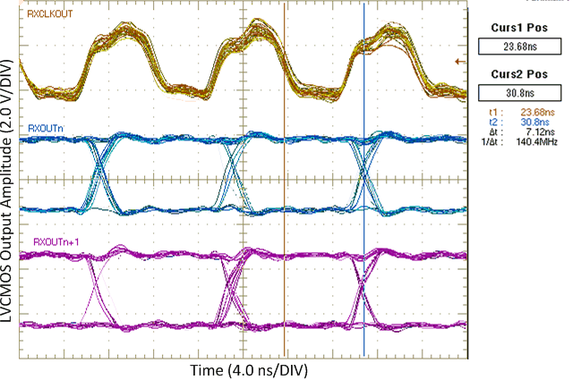
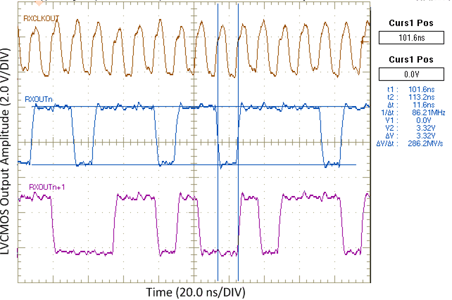
The following application curves are examples taken with a DS90C385A serializer interfacing to a DS90CF386 deserializer with nominal temperature (25ºC) and voltage supply (3.3 V) at an operating frequency of 85 MHz.
 Figure 24. LVDS RxIN0± Aligned With LVCMOS RxCLKOUT
 Figure 26. RxOUT Strobe On Falling Edge Of RxCLKOUT
 Figure 25. LVDS CLKIN Aligned With LVCMOS RxCLKOUT
 Figure 27. PRBS-7 Output On RxOUT Channels