SNLS209M November 2005 – January 2017 DS90C124 , DS90C241
PRODUCTION DATA.
- 1 Features
- 2 Applications
- 3 Description
- 4 Revision History
- 5 Pin Configuration and Functions
- 6 Specifications
- 7 Parameter Measurement Information
- 8 Detailed Description
- 9 Applications and Implementation
- 10Power Supply Recommendations
- 11Layout
- 12Device and Documentation Support
- 13Mechanical, Packaging, and Orderable Information
5 Pin Configuration and Functions
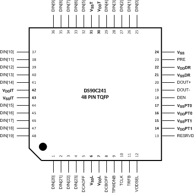
DS90C241 Serializer PFB Package
48-Pin TQFP
Top View

Pin Functions – DS90C241 Serializer
| PIN | TYPE(1) | DESCRIPTION | |
|---|---|---|---|
| NAME | NO. | ||
| LVCMOS PARALLEL INTERFACE PINS | |||
| DIN[23:0] | 4-1, 48-44, 41-32, 29-25 |
I | LVCMOS, Transmitter parallel interface data input pins. Tie LOW if unused, do not float. |
| TCLK | 10 | I | LVCMOS, Transmitter parallel interface clock input pin. Strobe edge set by TRFB configuration pin. |
| CONTROL AND CONFIGURATION PINS | |||
| DCAOFF | 5 | I | LVCMOS, Reserved. This pin must be tied LOW. |
| DCBOFF | 8 | I | LVCMOS, Reserved. This pin must be tied LOW. |
| DEN | 18 | I | LVCMOS, Transmitter data enable. DEN = H; LVDS driver outputs are enabled (ON). DEN = L; LVDS driver outputs are disabled (OFF), Transmitter LVDS driver DOUT (±) outputs are in TRI-STATE, PLL still operational and locked to TCLK. |
| PRE | 23 | I | LVCMOS, Pre-emphasis level select. PRE = NC (No Connect); Pre-emphasis is disabled (OFF). Pre-emphasis is active when input is tied to VSS through external resistor RPRE. Resistor value determines pre-emphasis level. Recommended value RPRE ≥ 3 kΩ; Imax = [(1.2/R) × 20], Rmin = 3 kΩ |
| RESRVD | 13 | I | LVCMOS, Reserved. This pin must be tied LOW. |
| TPWDNB | 9 | I | LVCMOS, Transmitter power down bar. TPWDNB = H; Transmitter is enabled and ON TPWDNB = L; Transmitter is in power down mode (Sleep), LVDS driver DOUT (±) outputs are in TRI-STATE stand-by mode, PLL is shutdown to minimize power consumption. |
| TRFB | 11 | I | LVCMOS, Transmitter clock edge select pin. TRFB = H; Parallel interface data is strobed on the rising clock edge. TRFB = L; Parallel interface data is strobed on the falling clock edge. |
| VODSEL | 12 | I | LVCMOS, VOD Level select VODSEL = L; LVDS driver output is approximately ± 400 mV (RL = 100 Ω) VODSEL = H; LVDS driver output is approximately ± 750 mV (RL = 100 Ω) For normal applications, set this pin LOW. For long cable applications where a larger VOD is required, set this pin HIGH. |
| LVDS SERIAL INTERFACE PINS | |||
| DOUT− | 19 | O | LVDS, Transmitter LVDS inverted (-) output This output is intended to be loaded with a 100-Ω load to the DOUT- pin. The interconnect must be AC-coupled to this pin with a 100-nF capacitor. |
| DOUT+ | 20 | O | LVDS, Transmitter LVDS true (+) output. This output is intended to be loaded with a 100-Ω load to the DOUT+ pin. The interconnect must be AC-coupled to this pin with a 100-nF capacitor. |
| POWER OR GROUND PINS | |||
| VDDDR | 22 | P | VDD, Analog voltage supply, LVDS output power |
| VDDIT | 42 | P | VDD, Digital voltage supply, Tx input power |
| VDDL | 7 | P | VDD, Digital voltage supply, Tx logic power |
| VDDPT0 | 16 | P | VDD, Analog voltage supply, VCO power |
| VDDPT1 | 14 | P | VDD, Analog voltage supply, PLL power |
| VDDT | 30 | P | VDD, Digital voltage supply, Tx serializer power |
| VSS | 24 | G | ESD ground |
| VSSDR | 21 | G | Analog ground, LVDS output ground |
| VSSIT | 43 | G | Digital ground, Tx input ground |
| VSSL | 6 | G | Digital ground, Tx logic ground |
| VSSPT0 | 17 | G | Analog ground, VCO ground |
| VSSPT1 | 15 | G | Analog ground, PLL ground |
| VSST | 31 | G | Digital ground, Tx serializer ground |
(1) G = Ground, I = Input, O = Output, P = Power
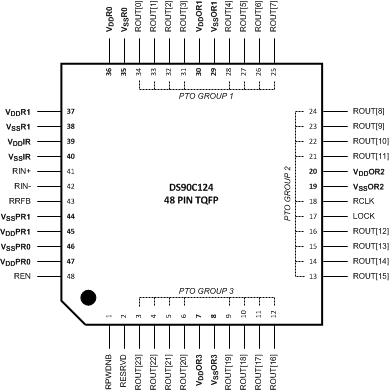
DS90C124 Deserializer PFB Package
48-Pin TQFP
Top View

Pin Functions – DS90C124 Deserializer
| PIN | TYPE(1) | DESCRIPTION | |
|---|---|---|---|
| NAME | NO. | ||
| LVCMOS PARALLEL INTERFACE PINS | |||
| RCLK | 18 | O | LVCMOS, Parallel interface clock output pin. Strobe edge set by RRFB configuration pin. |
| ROUT[7:0] | 25-28, 31-34 | O | LVCMOS, Receiver LVCMOS level outputs – Group 1 |
| ROUT[15:8] | 13-16, 21-24 | O | LVCMOS, Receiver LVCMOS level outputs – Group 2 |
| ROUT[23:16] | 3-6, 9-12 | O | LVCMOS, Receiver LVCMOS level outputs – Group 3 |
| CONTROL AND CONFIGURATION PINS | |||
| REN | 48 | I | LVCMOS, Receiver data enable REN = H; ROUT[23:0] and RCLK are enabled (ON). REN = L; ROUT[23:0] and RCLK are disabled (OFF), receiver ROUT[23:0] and RCLK outputs are in TRI-STATE, PLL still operational and locked to TCLK. |
| LOCK | 17 | O | LVCMOS, LOCK indicates the status of the receiver PLL LOCK = H; receiver PLL is locked LOCK = L; receiver PLL is unlocked, ROUT[23:0] and RCLK are TRI-STATED |
| RESRVD | 2 | I | LVCMOS, Reserved. This pin must be tied LOW. |
| RPWDNB | 1 | I | LVCMOS, Receiver power down bar. RPWDNB = H; Receiver is enabled and ON RPWDNB = L; Receiver is in power down mode (Sleep), ROUT[23:0], RCLK, and LOCK are in TRI-STATE standby mode, PLL is shutdown to minimize power consumption. |
| RRFB | 43 | I | LVCMOS, Receiver clock edge select pin. RRFB = H; ROUT LVCMOS outputs strobed on the rising clock edge. RRFB = L; ROUT LVCMOS outputs strobed on the falling clock edge. |
| LVDS SERIAL INTERFACE PINS | |||
| RIN− | 42 | I | Receiver LVDS Inverted (−) Input This input is intended to be terminated with a 100-Ω load to the RIN- pin. The interconnect must be AC-coupled to this pin with a 100-nF capacitor. |
| RIN+ | 41 | I | Receiver LVDS True (+) input This input is intended to be terminated with a 100-Ω load to the RIN+ pin. The interconnect must be AC-coupled to this pin with a 100-nF capacitor. |
| POWER OR GROUND PINS | |||
| VDDIR | 39 | P | VDD, Analog LVDS voltage supply, power |
| VDDOR1 | 30 | P | VDD, Digital voltage supply, LVCMOS output power |
| VDDOR2 | 20 | P | VDD, Digital voltage supply, LVCMOS output power |
| VDDOR3 | 7 | P | VDD, Digital voltage supply, LVCMOS output power |
| VDDPR0 | 47 | P | VDD, Analog voltage supply, PLL power |
| VDDPR1 | 45 | P | VDD, Analog voltage supply, PLL VCO power |
| VDDR0 | 36 | P | VDD, Digital voltage supply, Logic power |
| VDDR1 | 37 | P | VDD, Digital voltage supply, Logic power |
| VSSIR | 40 | G | Analog LVDS ground |
| VSSOR1 | 29 | G | Digital ground, LVCMOS output ground |
| VSSOR2 | 19 | G | Digital ground, LVCMOS output ground |
| VSSOR3 | 8 | G | Digital ground, LVCMOS output ground |
| VSSPR0 | 46 | G | Analog ground, PLL ground |
| VSSPR1 | 44 | G | Analog ground, PLL VCO ground |
| VSSR0 | 35 | G | Digital ground, Logic ground |
| VSSR1 | 38 | G | Digital ground, Logic ground |
(1) G = Ground, I = Input, O = Output, P = Power