SNLS209M November 2005 – January 2017 DS90C124 , DS90C241
PRODUCTION DATA.
- 1 Features
- 2 Applications
- 3 Description
- 4 Revision History
- 5 Pin Configuration and Functions
- 6 Specifications
- 7 Parameter Measurement Information
- 8 Detailed Description
- 9 Applications and Implementation
- 10Power Supply Recommendations
- 11Layout
- 12Device and Documentation Support
- 13Mechanical, Packaging, and Orderable Information
1 Features
- 5-MHz to 35-MHz Clock Embedded and DC-Balancing 24:1 and 1:24 Data Transmissions
- User Defined Pre-Emphasis Driving Ability Through External Resistor on LVDS Outputs and Capable to Drive Up to 10-Meter Shielded Twisted-Pair Cable
- User-Selectable Clock Edge for Parallel Data on Both Transmitter and Receiver
- Internal DC Balancing Encode and Decode (Supports AC-Coupling Interface With No External Coding Required)
- Individual Power-Down Controls for Both Transmitter and Receiver
- Embedded Clock CDR (Clock and Data Recovery) on Receiver and No External Source of Reference Clock Required
- All Codes RDL (Random Data Lock) to Support Live-Pluggable Applications
- LOCK Output Flag to Ensure Data Integrity at Receiver Side
- Balanced TSETUP and THOLD Between RCLK and RDATA on Receiver Side
- PTO (Progressive Turnon) LVCMOS Outputs to Reduce EMI and Minimize SSO Effects
- All LVCMOS Inputs and Control Pins Have Internal Pulldown
- On-Chip Filters for PLLs on Transmitter and Receiver
- Temperature Range: –40°C to 105°C
- Greater Than 8-kV HBM ESD Tolerant
- Meets AEC-Q100 Compliance
- Power Supply Range: 3.3 V ± 10%
- 48-Pin TQFP Package
2 Applications
- Automotive Central Information Displays
- Automotive Instrument Cluster Displays
- Automotive Heads-Up Displays
- Remote Camera-Based Driver Assistance Systems
3 Description
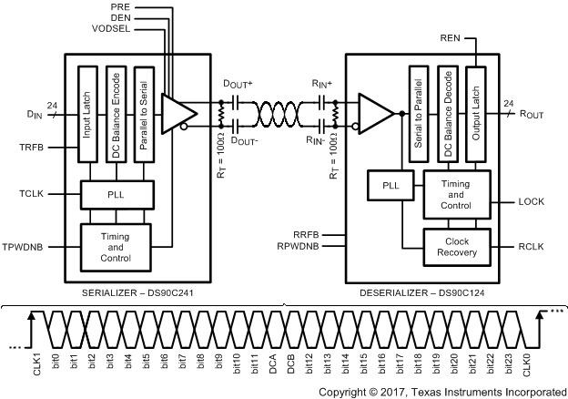
The DS90C241 and DS90C124 chipset translates a 24-bit parallel bus into a fully transparent data and control LVDS serial stream with embedded clock information. This single serial stream simplifies transferring a 24-bit bus over PCB traces or over cable by eliminating the skew problems between parallel data and clock paths. It saves system cost by narrowing data paths, which in turn reduces PCB layers, cable width, and connector size and pins.
The DS90C241 and DS90C124 incorporate LVDS signaling on the high-speed I/O. LVDS provides a low-power and low-noise environment for reliably transferring data over a serial transmission path. By optimizing the serializer output edge rate for the operating frequency range, EMI is further reduced.
In addition, the device features pre-emphasis to boost signals over longer distances using lossy cables. Internal DC balanced encoding and decoding supports AC-coupled interconnects.
Device Information(1)
| PART NUMBER | PACKAGE | BODY SIZE (NOM) |
|---|---|---|
| DS90C124 DS90C241 |
TQFP (48) | 7.00 mm x 7.00 mm |
- For all available packages, see the orderable addendum at the end of the data sheet.
Block Diagram

4 Revision History
Changes from L Revision (April 2013) to M Revision
- Added ESD Ratings table, Feature Description section, Device Functional Modes, Application and Implementation section, Power Supply Recommendations section, Layout section, Device and Documentation Support section, and Mechanical, Packaging, and Orderable Information sectionGo
- Deleted Lead temperature, soldering (260°C maximum) from Absolute Maximum RatingsGo
- Added Thermal Information tableGo
- Added Typical Characteristics (PCLK = 5 MHz and PCLK = 25 MHz plus pre-emphasis)Go
Changes from K Revision (April 2013) to L Revision
- Changed layout of National Semiconductor Data Sheet to TI formatGo