SNLS209M November 2005 – January 2017 DS90C124 , DS90C241
PRODUCTION DATA.
- 1 Features
- 2 Applications
- 3 Description
- 4 Revision History
- 5 Pin Configuration and Functions
- 6 Specifications
- 7 Parameter Measurement Information
- 8 Detailed Description
- 9 Applications and Implementation
- 10Power Supply Recommendations
- 11Layout
- 12Device and Documentation Support
- 13Mechanical, Packaging, and Orderable Information
9 Applications and Implementation
NOTE
Information in the following applications sections is not part of the TI component specification, and TI does not warrant its accuracy or completeness. TI’s customers are responsible for determining suitability of components for their purposes. Customers should validate and test their design implementation to confirm system functionality.
9.1 Application Information
9.1.1 Using the DS90C241 and DS90C124
The DS90C241/DS90C124 serializer or deserializer (SERDES) pair sends 24 bits of parallel LVCMOS data over a serial LVDS link up to 840 Mbps. Serialization of the input data is accomplished using an on-board PLL at the serializer which embeds clock with the data. The deserializer extracts the clock/control information from the incoming data stream and deserializes the data. The deserializer monitors the incoming clockl information to determine lock status and indicates lock by asserting the LOCK output high.
9.1.2 Display Application
The DS90C241/DS90C124 chipset is intended for interface between a host (graphics processor) and a display. It supports an 18-bit color depth (RGB666) and up to 800 × 480 display formats. In a RGB666 configuration 18 color bits (R[5:0], G[5:0], B[5:0]), Pixel Clock (PCLK) and three control bits (VS, HS, and DE) along with three spare bits are supported across the serial link with PCLK rates from 5 MHz to 35 MHz.
9.2 Typical Application
Figure 22 shows a typical application of the DS90C241 serializer (SER). The LVDS outputs use a 100-Ω termination and 100-nF coupling capacitors to the line. Bypass capacitors are placed near the power supply pins. A system General Purpose Output (GPO) controls the TPWDNB pin. In this application the TRFB pin is tied High to latch data on the rising edge of the TCLK. The DEN signal is not used and is tied High also. In this application, the link is short; therefore, the VODSEL pin is tied Low for the standard LVDS swing. The pre-emphasis input uses a resistor to ground to set the amount of pre-emphasis desired by the application.
Figure 23 shows a typical application of the DS90C124 deserializer (DES). The LVDS inputs use a 100-Ω termination and 100-nF coupling capacitors to the line. Bypass capacitors are placed near the power supply pins. A system GPO controls the RPWDNB pin. In this application, the RRFB pin is tied high to strobe the data on the rising edge of the RCLK. The REN signal is not used and is tied high also.
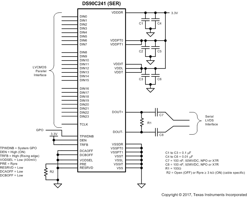 Figure 22. DS90C241 Typical Application Connection
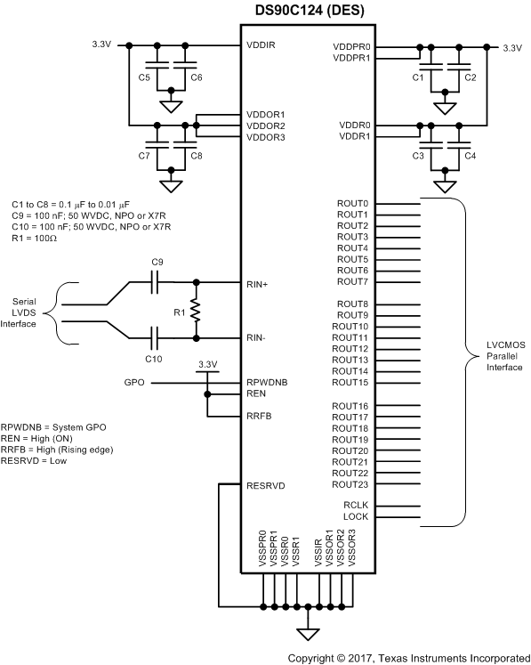 Figure 23. DS90C124 Tyical Application Connection
9.2.1 Design Requirements
For the typical design application, use the following as input parameters:
The SER/DES supports only AC-coupled interconnects through an integrated DC-balanced decoding scheme. External AC coupling capacitors must be placed in series in the FPD-Link III signal path as illustrated in Figure 22 and Figure 23.
9.2.2 Detailed Design Procedure
Circuit board layout and stack-up for the LVDS serializer and deserializer devices must be designed to provide low-noise power to the device. Good layout practice also separates high frequency or high-level inputs and outputs to minimize unwanted stray noise, feedback and interference. Power system performance may be greatly improved by using thin dielectrics (2 to 4 mil) for power and ground sandwiches. This arrangement uses the plane capacitance for the PCB power system and has low-inductance, which has proven effectiveness especially at high frequencies, and makes the value and placement of external bypass capacitors less critical. External bypass capacitors must include both RF ceramic and tantalum electrolytic types. RF capacitors may use values in the range of 0.01 µF to 10 µF. Tantalum capacitors may be in the 2.2-µF to 10-µF range. The voltage rating of the tantalum capacitors must be at least 5 times the power supply voltage being used.
MLCC surface mount capacitors are recommended due to their smaller parasitic properties. When using multiple capacitors per supply pin, place the smaller value closer to the pin. A large bulk capacitor is recommended at the point of power entry. This is typically in the 50 µF to 100 µF range and smooth low frequency switching noise. TI recommends connecting power and ground pins directly to the power and ground planes with bypass capacitors connected to the plane with through on both ends of the capacitor. Connecting power or ground pins to an external bypass capacitor will increase the inductance of the path. A small body size X7R chip capacitor, such as 0603 or 0805, is recommended for external bypass. A small body sized capacitor has less inductance. The user must pay attention to the resonance frequency of these external bypass capacitors, usually in the range from 20 MHz to 30 MHz. To provide effective bypassing, multiple capacitors are often used to achieve low impedance between the supply rails over the frequency of interest. At high frequency, it is also a common practice to use two vias from power and ground pins to the planes, reducing the impedance at high frequency. Use at least a four layer board with a power and ground plane. Place LVCMOS signals away from the LVDS lines to prevent coupling from the LVCMOS lines to the LVDS lines. Closely coupled differential lines of 100 Ω are typically recommended for LVDS interconnect. The closely coupled lines help to ensure that coupled noise will appear as common mode and thus is rejected by the receivers. The tightly coupled lines will also radiate less.
9.2.2.1 Noise Margin
The deserializer noise margin is the amount of input jitter (phase noise) that the deserializer can tolerate and still reliably recover data. Various environmental and systematic factors include:
- Serializer: TCLK jitter, VCC noise (noise bandwidth and out-of-band noise)
- Media: ISI, VCM noise
- Deserializer: VCC noise
For a graphical representation of noise margin, see Figure 18.
9.2.2.2 Transmission Media
The serializer and deserializer can be used in point-to-point configuration, through a PCB trace, or through twisted pair cable. In a point-to-point configuration, the transmission media requires termination at both ends of the transmitter and receiver pair. Interconnect for LVDS typically has a differential impedance of 100 Ω. Use cables and connectors that have matched differential impedance to minimize impedance discontinuities. In most applications that involve cables, the transmission distance is determined on data rates involved, acceptable bit error rate and transmission medium.
The resulting signal quality at the receiving end of the transmission media may be assessed by monitoring the differential eye opening of the serial data stream. The Receiver Input Tolerance in Switching Characteristics – Deserializer and the Differential Threshold Voltage specifications in Electrical Characteristics define the acceptable data eye opening. A differential probe must be used to measure across the termination resistor at the DS90C124 inputs. Figure 24 illustrates the eye opening and relationship to the receiver input tolerance and differential threshold voltage specifications.
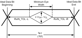 Figure 24. Receiver Input Eye Opening
9.2.2.3 Live Link Insertion
The serializer and deserializer devices support live pluggable applications. The automatic receiver lock to random data plug and go hot insertion capability allows the DS90C124 to attain lock to the active data stream during a live insertion event.
9.2.3 Application Curves
Figure 25, Figure 26, and Figure 27 are scope shots with PCLK = 25 MHz into the DS90C241 with a 1010... pattern on the DIN[23:0] inputs. The scope was triggered on the input PCLK.
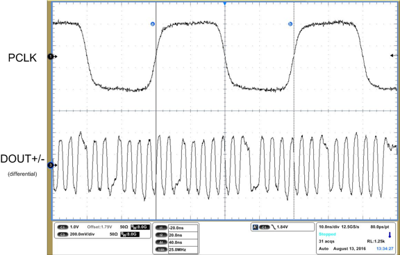 Figure 25. Input PCLK = 25 MHz and Associated DOUT Serial Stream
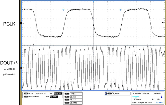 Figure 27. Input PCLK = 25 MHz and Associated DOUT Serial Stream With VODSEL = H
 Figure 26. Input PCLK = 25 MHz and Associated DOUT Serial Stream With Pre-Emphasis
Figure 28, Figure 29, and Figure 30 are scope shots with PCLK = 33 MHz into the DS90C241 with a 1010... pattern on the DIN[23:0] inputs. The scope was triggered on the input PCLK.
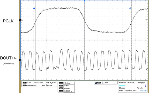 Figure 28. Input PCLK = 33 MHz and Associated DOUT Serial Stream
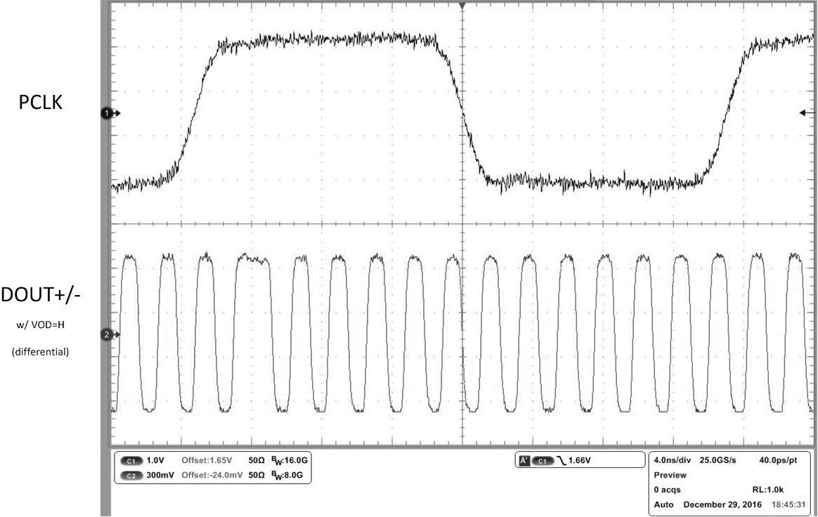 Figure 30. Input PCLK = 33 MHz and Associated DOUT Serial Stream With VODSEL = H
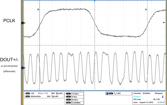 Figure 29. Input PCLK = 33 MHz and Associated DOUT Serial Stream With Pre-Emphasis