SNLS334G April 2011 – January 2015 DS80PCI800
PRODUCTION DATA.
- 1 Features
- 2 Applications
- 3 Description
- 4 Revision History
- 5 Pin Configuration and Functions
- 6 Specifications
- 7 Parameter Measurement Information
- 8 Detailed Description
- 9 Application and Implementation
- 10Power Supply Recommendations
- 11Layout
- 12Device and Documentation Support
- 13Mechanical, Packaging, and Orderable Information
5 Pin Configuration and Functions
DS80PCI800
54 Lead
Top View
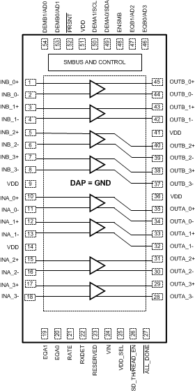
Pin Functions(1)(2)(3)(4)
| PIN | I/O, TYPE | DESCRIPTION | |
|---|---|---|---|
| NAME | NO. | ||
| DIFFERENTIAL HIGH SPEED I/Os | |||
| INB_0+, INB_0-, INB_1+, INB_1-, INB_2+, INB_2-, INB_3+, INB_3- | 1, 2, 3, 4, 5, 6, 7, 8 | I, CML | Inverting and non-inverting differential inputs to bank B equalizer. A gated on-chip 50-Ω termination resistor connects INB_n+ to VDD and INB_n- to VDD depending on the state of RXDET. See Table 4
AC coupling required on high-speed I/O |
| INA_0+, INA_0-, INA_1+, INA_1-, INA_2+, INA_2-, INA_3+, INA_3- | 10, 11, 12, 13, 15, 16, 17, 18 | I, CML | Inverting and non-inverting differential inputs to bank A equalizer. A gated on-chip 50-Ω termination resistor connects INA_n+ to VDD and INA_n- to VDD depending on the state of RXDET. See Table 4
AC coupling required on high-speed I/O |
| OUTB_0+, OUTB_0-, OUTB_1+, OUTB_1-, OUTB_2+, OUTB_2-, OUTB_3+, OUTB_3- | 45, 44, 43, 42, 40, 39, 38, 37 | O, CML | Inverting and non-inverting 50-Ω driver bank B outputs with de-emphasis. Compatible with AC-coupled CML inputs. |
| OUTA_0+, OUTA_0-, OUTA_1+, OUTA_1-, OUTA_2+, OUTA_2-, OUTA_3+, OUTA_3- | 35, 34, 33, 32, 31, 30, 29, 28 | O, CML | Inverting and non-inverting 50-Ω driver bank A outputs with de-emphasis. Compatible with AC-coupled CML inputs. |
| CONTROL PINS — SHARED (LVCMOS) | |||
| ENSMB | 48 | I, 4-LEVEL, LVCMOS | System management bus (SMBus) enable pin Tie 1 k to VDD (2.5-V mode) or VIN (3.3 V-mode) = Register access SMBus slave mode FLOAT = Read external EEPROM (master SMBUS mode) Tie 1 kΩ to GND = Pin mode |
| ENSMB = 1 (SMBus SLAVE MODE) | |||
| SCL | 50 | I, 2-LEVEL, LVCMOS, O, open drain | In SMBus Slave Mode, this pin is the SMBus clock I/O. Clock input or open drain output. External 2-kΩ to 5-kΩ pullup resistor to VDD or VIN recommended as per SMBus interface standards.(5) |
| SDA | 49 | I, 2-LEVEL, LVCMOS, O, open drain | In both SMBus Modes, this pin is the SMBus data I/O. Data input or open drain output. External 2-kΩ to 5-kΩ pullup resistor to VDD or VIN recommended as per SMBus interface standards.(5) |
| AD0-AD3 | 54, 53, 47, 46 | I, 4-LEVEL, LVCMOS | SMBus Slave Address Inputs. In both SMBus Modes, these pins are the user set SMBus slave address inputs. External 1-kΩ pullup or pulldown recommended. |
| READ_EN / SD_TH | 26 | I, FLOAT | In SMBus Slave Mode, this pin is not used. Leave it floating. |
| ENSMB = FLOAT (SMBus MASTER MODE) | |||
| SCL | 50 | I, 2-LEVEL, LVCMOS, O, open drain | Clock output when loading EEPROM configuration, reverting to SMBus clock input when EEPROM load is complete (ALL_DONE = 0). External 2-kΩ to 5-kΩ pullup resistor to VDD or VIN recommended as per SMBus interface standards.(5) |
| SDA | 49 | I, 2-LEVEL, LVCMOS, O, open drain | In both SMBus Modes, this pin is the SMBus data I/O. Data input or open drain output. External 2-kΩ to 5-kΩ pullup resistor to VDD or VIN recommended as per SMBus interface standards.(5) |
| AD0-AD3 | 54, 53, 47, 46 | I, 4-LEVEL, LVCMOS | SMBus Slave Address Inputs. In both SMBus Modes, these pins are the user set SMBus slave address inputs. External 1-kΩ pullup or pulldown recommended. |
| READ_EN | 26 | I, 2-LEVEL, LVCMOS | A logic low on this pin starts the load from the external EEPROM(6)
Once EEPROM load is complete (ALL_DONE = 0), this pin functionality remains as READ_EN. It does not revert to an SD_TH input. |
| ALL_DONE | 27 | O, 2-LEVEL, LVCMOS | Valid register load status output HIGH = External EEPROM load failed or incomplete LOW = External EEPROM load passed |
| ENSMB = 0 (PIN MODE) | |||
| EQA0, EQA1, EQB0, EQB1 |
20, 19, 46, 47 | I, 4-LEVEL, LVCMOS | EQA[1:0] and EQB[1:0] control the level of equalization on the input pins. The pins are active only when ENSMB is deasserted (low). The 8 channels are organized into two banks. Bank A is controlled with the EQA[1:0] pins and bank B is controlled with the EQB[1:0] pins. When ENSMB goes high the SMBus registers provide independent control of each channel. The EQB[1:0] pins are converted to SMBUS AD2/AD3 inputs. See Table 2. |
| DEMA0, DEMA1, DEMB0, DEMB1 |
49, 50, 53, 54 | I, 4-LEVEL, LVCMOS | DEMA[1:0] and DEMB[1:0] control the level of de-emphasis of the output driver. The pins are only active when ENSMB is deasserted (low). The 8 channels are organized into two banks. Bank A is controlled with the DEMA[1:0] pins and bank B is controlled with the DEMB[1:0] pins. When ENSMB goes high the SMBus registers provide independent control of each channel. The DEMA[1:0] pins are converted to SMBUS SCL/SDA and DEMB[1:0] pins are converted to AD0, AD1 inputs. See Table 3. |
| CONTROL PINS — BOTH PIN AND SMBUS MODES (LVCMOS) | |||
| RATE | 21 | I, 4-LEVEL, LVCMOS | RATE control pin selects GEN 1,2 and GEN 3 operating modes. Tie 1 kΩ to GND = GEN 1,2 FLOAT = AUTO Rate Select of Gen1/2 and Gen3 with de-emphasis Tie 20 kΩ to GND = GEN 3 without de-emphasis Tied 1 kΩ to VDD = RESERVED |
| RXDET | 22 | I, 4-LEVEL, LVCMOS | The RXDET pin controls the receiver detect function. Depending on the input level, a 50 Ω or > 50 kΩ termination to the power rail is enabled. See Table 4. |
| RESERVED | 23 | I, FLOAT | Float (leave pin open) = Normal Operation |
| VDD_SEL | 25 | I, LVCMOS | Controls the internal regulator FLOAT = 2.5-V mode Tie GND = 3.3-V mode See Figure 14 |
| SD_TH | 26 | I, 4-LEVEL, LVCMOS | Controls the internal Signal Detect Threshold. See Table 5. |
| PRSNT | 52 | I, 2-LEVEL, LVCMOS | Cable Present Detect input. High when a cable is not present per PCIe Cabling Spec. 1.0. Puts part into low power mode. When LOW (normal operation) part is enabled. See Table 4. |
| POWER | |||
| VIN | 24 | Power | In 3.3-V mode, feed 3.3 V to VIN In 2.5-V mode, leave floating |
| VDD | 9, 14, 36, 41, 51 | Power | Power supply pins 2.5-V mode, connect to 2.5-V supply 3.3-V mode, connect 0.1-µF capacitor to each VDD pin (output of LDO) |
| GND | DAP | Power | Ground pad (DAP - die attach pad) |
(1) LVCMOS inputs without the “FLOAT” conditions must be driven to a logic low or high at all times or operation is not verified.
(2) Input edge rate for LVCMOS/FLOAT inputs must be faster than 50 ns from 10% to 90%.
(3) For 3.3-V mode operation, VIN pin = 3.3 V and the VDD for the 4-level input is 3.3 V.
(4) For 2.5-V mode operation, VDD pin = 2.5 V and the VDD for the 4-level input is 2.5 V.
(5) SCL and SDA pins can be tied either to 3.3 V or 2.5 V, regardless of whether the device is operating in 2.5-V mode or 3.3-V mode.
(6) When READ_EN is asserted low, the device attempts to load EEPROM. If EEPROM cannot be loaded successfully, for example due to an invalid or blank hex file, the DS80PCI800 waits indefinitely in an unknown state where SMBus access is not possible. ALL_DONE pin remains high in this situation.