SNLS244H September 2006 – January 2016 DS42MB100
PRODUCTION DATA.
- 1 Features
- 2 Applications
- 3 Description
- 4 Revision History
- 5 Pin Configuration and Functions
- 6 Specifications
- 7 Parameter Measurement Information
- 8 Detailed Description
- 9 Application and Implementation
- 10Power Supply Recommendations
- 11Layout
- 12Device and Documentation Support
- 13Mechanical, Packaging, and Orderable Information
6 Specifications
6.1 Absolute Maximum Ratings
see(1)(2)| MIN | MAX | UNIT | |
|---|---|---|---|
| Supply voltage (VCC) | –0.3 | 4 | V |
| CMOS/TTL input voltage | –0.3 | VCC + 0.3 | V |
| CML input/output voltage | –0.3 | VCC + 0.3 | V |
| Junction temperature | 150 | °C | |
| Lead temperature (soldering, 4 seconds) | 260 | °C | |
| Storage temperature, Tstg | –65 | 150 | °C |
(1) Stresses beyond those listed under Absolute Maximum Ratings may cause permanent damage to the device. These are stress ratings only, which do not imply functional operation of the device at these or any other conditions beyond those indicated under Recommended Operating Conditions. Exposure to absolute-maximum-rated conditions for extended periods may affect device reliability.
(2) If Military/Aerospace specified devices are required, please contact the TI Sales Office/Distributors for availability and specifications.
6.2 ESD Ratings
| VALUE | UNIT | |||
|---|---|---|---|---|
| V(ESD) | Electrostatic discharge | Human-body model (HBM), 1.5 kΩ, 100 pF, per ANSI/ESDA/JEDEC JS-001(1) | ±6000 | V |
| Charged-device model (CDM), per JEDEC specification JESD22-C101(2) | ±1250 | |||
| Machine model | ±350 | |||
(1) JEDEC document JEP155 states that 500-V HBM allows safe manufacturing with a standard ESD control process.
(2) JEDEC document JEP157 states that 250-V CDM allows safe manufacturing with a standard ESD control process.
6.3 Recommended Operating Ratings
| MIN | NOM | MAX | UNIT | |
|---|---|---|---|---|
| Supply voltage (VCC – GND) | 3.135 | 3.3 | 3.465 | V |
| Supply noise amplitude (10 Hz to 2 GHz) | 100 | mVPP | ||
| Ambient temperature | –40 | 85 | °C | |
| Case temperature | 100 | °C |
6.4 Thermal Information
| THERMAL METRIC(1) | DS42MB100 | UNIT | |
|---|---|---|---|
| NJK (WQFN) | |||
| 36 PINS | |||
| RθJA | Junction-to-ambient thermal resistance(2) | 32.8 | °C/W |
| RθJC(top) | Junction-to-case (top) thermal resistance | 14.3 | °C/W |
| RθJB | Junction-to-board thermal resistance | 6.2 | °C/W |
| ψJT | Junction-to-top characterization parameter | 0.2 | °C/W |
| ψJB | Junction-to-board characterization parameter | 6.1 | °C/W |
| RθJC(bot) | Junction-to-case (bottom) thermal resistance | 1.9 | °C/W |
(1) For more information about traditional and new thermal metrics, see the Semiconductor and IC Package Thermal Metrics application report, SPRA953.
(2) Thermal resistances are based on having 16 thermal relief vias on the DAP pad under the 0 airflow condition.
6.5 Electrical Characteristics
Over recommended operating supply and temperature ranges unless otherwise specified.| PARAMETER | TEST CONDITIONS | MIN | TYP(1) | MAX | UNIT | ||
|---|---|---|---|---|---|---|---|
| LVCMOS DC SPECIFICATIONS | |||||||
| VIH | High level input voltage | 2 | VCC + 0.3 | V | |||
| VIL | Low level input voltage | –0.3 | 0.8 | V | |||
| IIH | High level input current | VIN = VCC | –10 | 10 | µA | ||
| IIL | Low level input current | VIN = GND | 75 | 94 | 124 | µA | |
| RPU | Pull-high resistance | 35 | kΩ | ||||
| RECEIVER SPECIFICATIONS | |||||||
| VID | Differential input voltage range(2) | AC coupled differential signal. This parameter is not tested at production. |
Below 1.25 Gbps | 100 | 1750 | mVP-P | |
| Between 1.25 Gbps–3.125 Gbps | 100 | 1560 | |||||
| Above 3.125 Gbps | 100 | 1200 | |||||
| VICM | Common-mode voltage at receiver inputs | Measured at receiver inputs reference to ground. | 1.3 | V | |||
| RITD | Input differential termination(3) | On-chip differential termination between IN+ or IN−. | 84 | 100 | 116 | Ω | |
| DRIVER SPECIFICATIONS | |||||||
| VODB | Output differential voltage swing without pre-emphasis(4) | RL = 100 Ω ±1% DES_1 = DES_0 = 0 DEL_1 = DEL_0 = 0 Driver pre-emphasis disabled. Running K28.7 pattern at 4.25 Gbps. See Figure 6 for test circuit. |
1100 | 1300 | 1500 | mVP-P | |
| VPE | Output pre-emphasis voltage ratio 20 × log (VODPE / VODB) |
RL = 100 Ω ±1% Running K28.7 pattern at 4.25 Gbps x = S for switch side pre-emphasis control x = L for line side pre-emphasis control See Figure 9 on waveform. See Figure 6 for test circuit. |
DEx_[1:0] = 00 | 0 | dB | ||
| DEx_[1:0] = 01 | –3 | ||||||
| DEx_[1:0] = 10 | –6 | ||||||
| DEx_[1:0] = 11 | –9 | ||||||
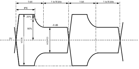
| TPE | Pre-emphasis width | Tested at −9-dB pre-emphasis level, DEx[1:0] = 11 x = S for switch side pre-emphasis control x = L for line side pre-emphasis control See Figure 3 on measurement condition. |
125 | 188 | 250 | ps | |
| ROTSE | Output termination(3) | On-chip termination from OUT+ or OUT− to VCC | 42 | 50 | 58 | Ω | |
| ROTD | Output differential termination | On-chip differential termination between OUT+ and OUT− | 100 | Ω | |||
| ΔROTSE | Mismatch in output termination resistors | Mismatch in output terminations at OUT+ and OUT− | 5% | ||||
| VOCM | Output common mode voltage | 2.7 | V | ||||
| POWER DISSIPATION | |||||||
| PD | Power dissipation | VDD = 3.3 V at 25°C All outputs terminated by 100 Ω ±1%. DEL_[1:0] = 0, DES_[1:0] = 0 Running PRBS 27– 1 pattern at 4.25 Gbps |
0.45 | W | |||
| AC CHARACTERISTICS | |||||||
| RJ | Device random jitter(5) | See Figure 6 for test circuit. Alternating 1-0 pattern. EQ and pre-emphasis disabled. |
At 0.25 Gbps | 2 | psrms | ||
| At 1.25 Gbps | 2 | ||||||
| At 4.25 Gbps | 2 | ||||||
| DJ | Device deterministic jitter(6) | See Figure 6 for test circuit. EQ and pre-emphasis disabled |
Between 0.25 and 4.25 Gbps with PRBS7 pattern for DS42MB100 at –40°C to 85°C |
35 | psp-p | ||
| DR | Data rate(2) | Tested with alternating 1-0 pattern | 0.25 | 4.25 | Gbps | ||
(1) Typical parameters measured at VCC = 3.3 V, TA = 25°C, and represent most likely parametric norms at the time of product characterization. The typical specifications are not ensured.
(2) This parameter is specified by design and/or characterization. It is not tested in production.
(3) IN+ and IN− are generic names refer to one of the many pairs of complimentary inputs of the DS42MB100. OUT+ and OUT− are generic names refer to one of the many pairs of the complimentary outputs of the DS42MB100. Differential input voltage VID is defined as |IN+–IN−|. Differential output voltage VOD is defined as |OUT+–OUT−|.
(4) K28.7 pattern is a 10-bit repeating pattern of K28.7 code group {001111 1000} K28.5 pattern is a 20-bit repeating pattern of +K28.5 and −K28.5 code groups {110000 0101 001111 1010}
(5) Device output random jitter is a measurement of the random jitter contribution from the device. It is derived by the equation sqrt(RJOUT2 – RJIN2), where RJOUT is the total random jitter measured at the output of the device in psrms, RJIN is the random jitter of the pattern generator driving the device.
(6) Device output deterministic jitter is a measurement of the deterministic jitter contribution from the device. It is derived by the equation (DJOUT – DJIN), where DJOUT is the total peak-to-peak deterministic jitter measured at the output of the device in psp-p, DJIN is the peak-to-peak deterministic jitter of the pattern generator driving the device.
6.6 Switching Characteristics
over operating free-air temperature range (unless otherwise noted)| PARAMETER | TEST CONDITIONS | MIN | TYP | MAX | UNIT | |
|---|---|---|---|---|---|---|
| tR | Differential low to high transition time | Measured with a clock-like pattern at 4.25 Gbps, between 20% and 80% of the differential output voltage. Pre-emphasis disabled. Transition time is measured with fixture as shown in Figure 6, adjusted to reflect the transition time at the output pins. |
85 | ps | ||
| tF | Differential high to low transition time | 85 | ps | |||
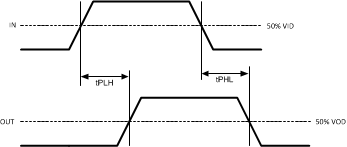
| tPLH | Differential low to high propagation delay | Measured at 50% differential voltage from input to output. | 1 | ns | ||
| tPHL | Differential high to low propagation delay | 1 | ns | |||
| tSKP | Pulse skew | |tPHL – tPLH| | 20 | ps | ||
| tSKO | Output skew(1) | Difference in propagation delay among data paths in the same device. | 100 | ps | ||
| tSKPP | Part-to-part skew | Difference in propagation delay between the same output from devices operating under identical condition. | 100 | ps | ||
| tSM | MUX switch time | Measured from VIH or VIL of the MUX-control or loopback control to 50% of the valid differential output. | 1.8 | 6 | ns | |
(1) tSKO is the magnitude difference in the propagation delays among data paths. An example is the output skew among data paths from IN0± to OUT± and IN1± to OUT±.. Another example is the output skew among data paths from IN± to OUT0± and IN± to OUT1±. tSKO also refers to the delay skew of the loopback paths of the same port and between similar data paths. An example is the output skew among data paths IN0± to OUT0± and IN1± to OUT1±.
 Figure 1. Driver Output Transition Time
 Figure 2. Propagation Delay From Input To Output
 Figure 3. Test Condition For Output Pre-Emphasis Duration
6.7 Typical Characteristics
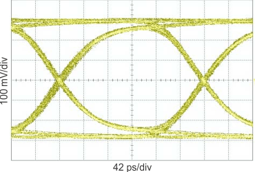
 Figure 4. PRBS-7, Pre-Emphasis = 0 dB at 4 Gbps
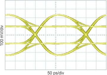
 Figure 5. PRBS-7, Pre-Emphasis = –9 dB at 4 Gbps