SNLS244H September 2006 – January 2016 DS42MB100
PRODUCTION DATA.
- 1 Features
- 2 Applications
- 3 Description
- 4 Revision History
- 5 Pin Configuration and Functions
- 6 Specifications
- 7 Parameter Measurement Information
- 8 Detailed Description
- 9 Application and Implementation
- 10Power Supply Recommendations
- 11Layout
- 12Device and Documentation Support
- 13Mechanical, Packaging, and Orderable Information
8 Detailed Description
8.1 Overview
The DS42MB100 is a signal conditioning 2:1 multiplexer and a 1:2 buffer designed to support port redundancy with encoded or scrambled data rates between 0.25 and 4.25 Gbps. The DS42MB100 provides fixed equalization at the receive input and pre-emphasis control on the output in order to support signal reach extension.
8.2 Functional Block Diagram
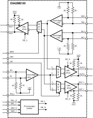
 Figure 7. Simplified Block Diagram
8.3 Feature Description
The DS42MB100 MUX buffer consists of several key blocks:
- CML Inputs and EQ
- Multiplexer and Loopback Control
- CML Drivers and Pre-Emphasis Control
CML inputs and EQ
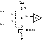
The high speed inputs are self-biased to about 1.3 V at IN+ and IN- and are designed for AC coupling, allowing the DS42MB100 to be inserted directly into the datapath without any limitation. See Figure 8 for details about the internal receiver input termination and bias circuit.
 Figure 8. Receiver Input Termination and Bias Circuit
The inputs are compatible to most AC coupling differential signals such as LVDS, LVPECL, and CML. The ideal AC coupling capacitor value is often based on the lowest frequency component embedded within the serial link. A typical AC coupling capacitor value ranges between 100 and 1000 nF. Some specifications with scrambled data may require a larger coupling capacitor for optimal performance. To reduce unwanted parasitics around and within the AC coupling capacitor, a body size of 0402 is recommended. Figure 6 shows the AC coupling capacitor placement in an AC test circuit.
Each input stage has a fixed equalizer that provides equalization to compensate about 5 dB (at 2 GHz) of transmission loss from a short backplane trace (about 10 inches backplane). EQ can be enabled or disabled with the EQL and EQS pins.
Table 1. EQ Controls for Line and Switch Inputs
| PIN | PIN VALUE | EQUALIZER FUNCTION |
|---|---|---|
| EQL, EQS | 0 | Enable equalization. |
| 1 (default) | Normal mode. Equalization disabled. |
Multiplexer and Loopback Control
Table 2 and Table 3 provide details about how to configure the DS42MB100 multiplexer and loopback settings.
Table 2. Logic Table for Multiplex Controls
| PIN | PIN VALUE | MUX FUNCTION |
|---|---|---|
| MUX | 0 | MUX select switch input IN1±. |
| 1 (default) | MUX select switch input IN0±. |
Table 3. Logic Table for Loopback Controls
| PIN | PIN VALUE | LOOPBACK FUNCTION |
|---|---|---|
| LB0 | 0 | Enable loopback from IN0± to OUT0±. |
| 1 (default) | Normal mode. Loopback disabled. | |
| LB1 | 0 | Enable loopback from IN1± to OUT1±. |
| 1 (default) | Normal mode. Loopback disabled. |
8.3.1 CML Drivers and Pre-Emphasis Control
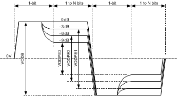
The output driver has pre-emphasis (driver-side equalization) to compensate the transmission loss of the backplane that it is driving. The driver conditions the output signal such that the lower frequency and higher frequency pulses reach approximately the same amplitude at the end of the backplane and minimize the deterministic jitter caused by the amplitude disparity. The DS42MB100 provides four steps of user-selectable pre-emphasis ranging from 0, –3, –6 and –9 dB to handle different lengths of backplane. Figure 9 shows a driver pre-emphasis waveform. The pre-emphasis duration is 188 ps nominal, corresponding to 0.8 unit intervals (UI) at 4.25 Gbps. The pre-emphasis levels of switch-side and line-side can be individually programmed.
 Figure 9. Driver Pre-Emphasis Differential Waveform (Showing All 4 Pre-Emphasis Steps)
Table 4. Line-Side Pre-Emphasis Controls
| DEL_[1:0] | PRE-EMPHASIS LEVEL IN mVPP
(VODB) |
PRE-EMPHASIS LEVEL IN mVPP
(VODPE) |
PRE-EMPHASIS IN dB (VODPE/VODB) |
TYPICAL FR4 BOARD TRACE |
|---|---|---|---|---|
| 0 0 | 1300 | 1300 | 0 | 10 inches |
| 0 1 | 1300 | 920 | −3 | 20 inches |
| 1 0 | 1300 | 650 | −6 | 30 inches |
| 1 1 (default) |
1300 | 461 | −9 | 40 inches |
Table 5. Switch-Side Pre-Emphasis Controls
| DES_[1:0] | PRE-EMPHASIS LEVEL IN mVPP
(VODB) |
PRE-EMPHASIS LEVEL IN mVPP
(VODPE) |
PRE-EMPHASIS IN dB (VODPE/VODB) |
TYPICAL FR4 BOARD TRACE |
|---|---|---|---|---|
| 0 0 | 1300 | 1300 | 0 | 10 inches |
| 0 1 | 1300 | 920 | −3 | 20 inches |
| 1 0 | 1300 | 650 | −6 | 30 inches |
| 1 1 (default) |
1300 | 461 | −9 | 40 inches |