ZHCSKE8D March 2016 – October 2019 DS250DF410
PRODUCTION DATA.
- 1 特性
- 2 应用
- 3 说明
- 4 修订历史记录
- 5 说明 (续)
- 6 Pin Configuration and Functions
-
7 Specifications
- 7.1 Absolute Maximum Ratings
- 7.2 ESD Ratings
- 7.3 Recommended Operating Conditions
- 7.4 Thermal Information
- 7.5 Electrical Characteristics
- 7.6 Timing Requirements, Retimer Jitter Specifications
- 7.7 Timing Requirements, Retimer Specifications
- 7.8 Timing Requirements, Recommended Calibration Clock Specifications
- 7.9 Recommended SMBus Switching Characteristics (Slave Mode)
- 7.10 Recommended SMBus Switching Characteristics (Master Mode)
- 7.11 Recommended JTAG Switching Characteristics
- 7.12 Typical Characteristics
-
8 Detailed Description
- 8.1 Overview
- 8.2 Functional Block Diagram
- 8.3
Feature Description
- 8.3.1 Device Data Path Operation
- 8.3.2 Signal Detect
- 8.3.3 Continuous Time Linear Equalizer (CTLE)
- 8.3.4 Variable Gain Amplifier (VGA)
- 8.3.5 Cross-Point Switch
- 8.3.6 Decision Feedback Equalizer (DFE)
- 8.3.7 Clock and Data Recovery (CDR)
- 8.3.8 Calibration Clock
- 8.3.9 Differential Driver with FIR Filter
- 8.3.10 Debug Features
- 8.3.11 Interrupt Signals
- 8.3.12 JTAG Boundary Scan
- 8.4 Device Functional Modes
- 8.5 Programming
- 8.6 Register Maps
- 9 Application and Implementation
- 10Power Supply Recommendations
- 11Layout
- 12器件和文档支持
- 13机械、封装和可订购信息
9.2.1.3 Application Curves
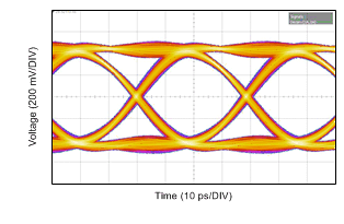
 Figure 18. DS250DF410 Operating at 25.78125 Gbps
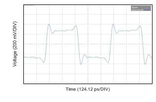
  Figure 19. DS250DF410 FIR Transmit Equalization While Operating at 25.78125 Gbps
 Figure 18 shows a typical output eye diagram for the DS250DF410 operating at 25.78125 Gbps with PRBS9 pattern using FIR main-cursor of +18, pre-cursor of -1 and post-cursor of +2. All other device settings are left at default.
Figure 19 shows an example of DS250DF410 FIR transmit equalization while operating at 25.78125 Gbps. In this example, the Tx FIR filter main-cursor is set to +15, post-cursor to -3 and pre-cursor to -3. An 8T pattern is used to evaluate the FIR filter, which consists of 0xFF00. All other device settings are left at default.