SLVSBN4C January   2013  – August 2016 DRV8839

PRODUCTION DATA.  

  1. Features
  2. Applications
  3. Description
  4. Revision History
  5. Pin Configuration and Functions
  6. Specifications
    1. 6.1 Absolute Maximum Ratings
    2. 6.2 ESD Ratings
    3. 6.3 Recommended Operating Conditions
    4. 6.4 Thermal Information
    5. 6.5 Electrical Characteristics
    6. 6.6 Timing Requirements
    7. 6.7 Typical Characteristics
  7. Detailed Description
    1. 7.1 Overview
    2. 7.2 Functional Block Diagram
    3. 7.3 Feature Description
      1. 7.3.1 Protection Circuits
        1. 7.3.1.1 Overcurrent Protection (OCP)
        2. 7.3.1.2 Thermal Shutdown (TSD)
        3. 7.3.1.3 Undervoltage Lockout (UVLO)
    4. 7.4 Device Functional Modes
      1. 7.4.1 Bridge Control
      2. 7.4.2 Sleep Mode
      3. 7.4.3 Motor Connections
  8. Application and Implementation
    1. 8.1 Application Information
    2. 8.2 Typical Application
      1. 8.2.1 Design Requirements
      2. 8.2.2 Detailed Design Procedure
        1. 8.2.2.1 Motor Voltage
        2. 8.2.2.2 Low-Power Operation
        3. 8.2.2.3 Application Curves
  9. Power Supply Recommendations
    1. 9.1 Bulk Capacitance
  10. 10Layout
    1. 10.1 Layout Guidelines
    2. 10.2 Layout Example
    3. 10.3 Thermal Considerations
      1. 10.3.1 Power Dissipation
  11. 11Device and Documentation Support
    1. 11.1 Documentation Support
      1. 11.1.1 Related Documentation
    2. 11.2 Receiving Notification of Documentation Updates
    3. 11.3 Community Resources
    4. 11.4 Trademarks
    5. 11.5 Electrostatic Discharge Caution
    6. 11.6 Glossary
  12. 12Mechanical, Packaging, and Orderable Information

封装选项

机械数据 (封装 | 引脚)
散热焊盘机械数据 (封装 | 引脚)
订购信息

9 Power Supply Recommendations

The input pins can drive within their recommended operating conditions with or without the VCC and VM power supplies present. No leakage current path exists to the supply. There is a weak pulldown resistor (approximately 100 kΩ) to ground on each input pin.

VCC and VM can be applied and removed in any order. When VCC is removed, the device enters a low-power state and draws very little current from VM. If the supply voltage is between 1.8 V and 7 V, VCC and VM can connect together.

The VM voltage supply does not have any undervoltage lockout protection (UVLO), so as long as VCC > 1.8 V, the internal device logic remains active. This means that the VM pin voltage may drop to 0 V, however, the load may not be sufficiently driven at low VM voltages.

9.1 Bulk Capacitance

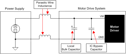
Having appropriate local bulk capacitance is an important factor in motor drive system design. It is generally beneficial to have more bulk capacitance, while the disadvantages are increased cost and physical size.

The required amount of local capacitance depends on a variety of factors, including:

  • The highest current required by the motor system
  • The power supply’s capacitance and ability to source current
  • The amount of parasitic inductance between the power supply and motor system
  • The acceptable voltage ripple
  • The type of motor used (brushed DC, brushless DC, stepper)
  • The motor braking method
DRV8839 bulk_cap_slvsbn4.gif Figure 12. Bulk Capacitance