SLVSBN4C January   2013  – August 2016 DRV8839

PRODUCTION DATA.  

  1. Features
  2. Applications
  3. Description
  4. Revision History
  5. Pin Configuration and Functions
  6. Specifications
    1. 6.1 Absolute Maximum Ratings
    2. 6.2 ESD Ratings
    3. 6.3 Recommended Operating Conditions
    4. 6.4 Thermal Information
    5. 6.5 Electrical Characteristics
    6. 6.6 Timing Requirements
    7. 6.7 Typical Characteristics
  7. Detailed Description
    1. 7.1 Overview
    2. 7.2 Functional Block Diagram
    3. 7.3 Feature Description
      1. 7.3.1 Protection Circuits
        1. 7.3.1.1 Overcurrent Protection (OCP)
        2. 7.3.1.2 Thermal Shutdown (TSD)
        3. 7.3.1.3 Undervoltage Lockout (UVLO)
    4. 7.4 Device Functional Modes
      1. 7.4.1 Bridge Control
      2. 7.4.2 Sleep Mode
      3. 7.4.3 Motor Connections
  8. Application and Implementation
    1. 8.1 Application Information
    2. 8.2 Typical Application
      1. 8.2.1 Design Requirements
      2. 8.2.2 Detailed Design Procedure
        1. 8.2.2.1 Motor Voltage
        2. 8.2.2.2 Low-Power Operation
        3. 8.2.2.3 Application Curves
  9. Power Supply Recommendations
    1. 9.1 Bulk Capacitance
  10. 10Layout
    1. 10.1 Layout Guidelines
    2. 10.2 Layout Example
    3. 10.3 Thermal Considerations
      1. 10.3.1 Power Dissipation
  11. 11Device and Documentation Support
    1. 11.1 Documentation Support
      1. 11.1.1 Related Documentation
    2. 11.2 Receiving Notification of Documentation Updates
    3. 11.3 Community Resources
    4. 11.4 Trademarks
    5. 11.5 Electrostatic Discharge Caution
    6. 11.6 Glossary
  12. 12Mechanical, Packaging, and Orderable Information

封装选项

机械数据 (封装 | 引脚)
散热焊盘机械数据 (封装 | 引脚)
订购信息

5 Pin Configuration and Functions

DSS Package
12-Pin WSON With Exposed Thermal Pad
Top View
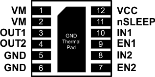
DRV8839 po_lvsbn4.gif

Pin Functions

PIN I/O (1) DESCRIPTION EXTERNAL COMPONENTS
OR CONNECTIONS
NAME NO.
POWER AND GROUND
GND, Thermal pad 5, 6 Device ground
VCC 12 Device supply Bypass to GND with a 0.1-μF, 6.3-V ceramic capacitor
VM 1, 2 Motor supply Bypass to GND with a 0.1-μF, 16-V ceramic capacitor
CONTROL
EN1 9 I Enable 1 Logic high enables OUT1
Internal pulldown resistor
EN2 7 I Enable 2 Logic high enables OUT2
Internal pulldown resistor
IN1 10 I Input 1 Logic input controls OUT1
Internal pulldown resistor
IN2 8 I Input 2 Logic input controls OUT2
Internal pulldown resistor
nSLEEP 11 I Sleep mode input Logic low puts device in low-power sleep mode
Logic high for normal operation
Internal pulldown resistor
OUTPUT
OUT1 3 O Output 1 Connect to motor winding
OUT2 4 O Output 2
(1) Directions: I = input, O = output, OZ = tri-state output, OD = open-drain output, IO = input/output.