SLVSBN4C January 2013 – August 2016 DRV8839
PRODUCTION DATA.
10 Layout
10.1 Layout Guidelines
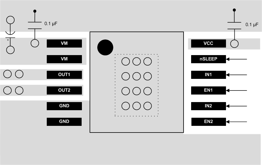
The VCC pin should be bypassed to GND using low-ESR ceramic bypass capacitors with a recommended value of 0.1-μF rated for VCC. This capacitor should be placed as close to the VCC pin as possible with a thick trace.
The VM pin should be bypassed to GND using low-ESR ceramic bypass capacitors with a recommended value of 0.1 μF rated for VM. This capacitor should be placed as close to the VM pin as possible with a thick trace. The VM pin must bypass to ground using an appropriate bulk capacitor. This component can be an electrolytic and should be located close to the DRV8839 device.
10.3 Thermal Considerations
The DRV8839 has thermal shutdown (TSD) as described above. If the die temperature exceeds approximately 150°C, the device disables until the temperature drops to a safe level.
Any tendency of the device to enter thermal shutdown is an indication of either excessive power dissipation, insufficient heatsinking, or too high an ambient temperature.
10.3.1 Power Dissipation
The power dissipation of the DRV8839 is a function of RMS motor current and the each output’s FET resistance (RDS(ON)) as seen in Equation 1:
For this example, VVM = 1.8 V, VVCC = 1.8 V, the ambient temperature is 35°C, and the junction temperature reaches 65°C. At 65°C, the sum of RDS(ON) is about 1 Ω. With an example motor current of 0.8 A, the dissipated power in the form of heat will be 0.8 A² × 1 Ω = 0.64 W.
The temperature that the DRV8839 reaches will depend on the thermal resistance to the air and PCB. It is important to solder the device thermal pad to the PCB ground plane, with vias to the top and bottom board layers, in order dissipate heat into the PCB and reduce the device temperature. In the example used here, the DRV8839 had an effective thermal resistance RθJA of 47°C/W, and as shown in Equation 2:
