ZHCSFB2A July 2016 – July 2016 DRV8837C
PRODUCTION DATA.
7 Detailed Description
7.1 Overview
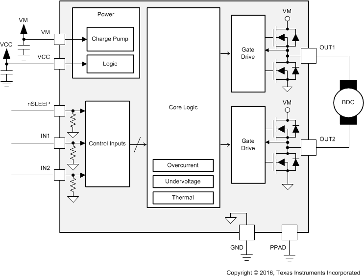
The DRV8837C device is an H-bridge driver that can drive one DC motor or other devices like solenoids. The outputs are controlled using a PWM interface (IN1/IN2).
A low-power sleep mode is included, which can be enabled using the nSLEEP pin.
This device greatly reduces the component count of motor driver systems by integrating the necessary driver FETs and FET control circuitry into a single device. In addition, the DRV8837C device adds protection features beyond traditional discrete implementations: undervoltage lockout, overcurrent protection, and thermal shutdown.
7.2 Functional Block Diagram

7.3 Feature Description
7.3.1 Bridge Control
The DRV8837C device is controlled using a PWM input interface, also called an IN/IN interface. Each output is controlled by a corresponding input pin.
Table 1 shows the logic for the DRV8837C device.
Table 1. DRV8837C Device Logic
| nSLEEP | IN1 | IN2 | OUT1 | OUT2 | FUNCTION (DC MOTOR) |
|---|---|---|---|---|---|
| 0 | X | X | Z | Z | Coast |
| 1 | 0 | 0 | Z | Z | Coast |
| 1 | 0 | 1 | L | H | Reverse |
| 1 | 1 | 0 | H | L | Forward |
| 1 | 1 | 1 | L | L | Brake |
7.3.2 Sleep Mode
If the nSLEEP pin is brought to a logic-low state, the DRV8837C device enters a low-power sleep mode. In this state, all unnecessary internal circuitry is powered down.
7.3.3 Power Supplies and Input Pins
The input pins can be driven within the recommended operating conditions with or without the VCC, VM, or both power supplies present. No leakage current path exists to the supply. Each input pin has a weak pulldown resistor (approximately 100 kΩ) to ground.
The VCC and VM supplies can be applied and removed in any order. When the VCC supply is removed, the device enters a low-power state and draws very little current from the VM supply. The VCC and VM pins can be connected together if the supply voltage is between 1.8 and 7 V.
The VM voltage supply does not have any undervoltage-lockout protection (UVLO). As long as VCC > 1.8 V, the internal device logic remains active which means that the VM pin voltage can drop to 0 V, however, the load may not be sufficiently driven at low VM voltages.
7.3.4 Protection Circuits
The DRV8837C is fully protected against VCC undervoltage, overcurrent, and overtemperature events.
-
VCC undervoltage lockout If at any time the voltage on the VCC pin falls below the undervoltage lockout threshold voltage, all FETs in the H-bridge are disabled. Operation resumes when the VCC pin voltage rises above the UVLO threshold.
-
Overcurrent protection (OCP) An analog current-limit circuit on each FET limits the current through the FET by removing the gate drive. If this analog current limit persists for longer than tDEG, all FETs in the H-bridge are disabled. Operation resumes automatically after tRETRY has elapsed. Overcurrent conditions are detected on both the high-side and low-side devices. A short to the VM pin, GND, or from the OUT1 pin to theOUT2 pin results in an overcurrent condition.
-
Thermal shutdown (TSD) If the die temperature exceeds safe limits, all FETs in the H-bridge are disabled. After the die temperature falls to a safe level, operation automatically resumes.
Table 2. Fault Behavior
| FAULT | CONDITION | H-BRIDGE | RECOVERY |
|---|---|---|---|
| VCC undervoltage (UVLO) | VCC < 1.7 V | Disabled | VCC > 1.8 V |
| Overcurrent (OCP) | IOUT > 1.2 A (MIN) | Disabled (retries automatically) | tRETRY elapses |
| Thermal Shutdown (TSD) | TJ > 150°C (MIN) | Disabled (retries automatically) | TJ < 150°C |
7.4 Device Functional Modes
The DRV8837C device is active unless the nSLEEP pin is brought logic low. In sleep mode the H-bridge FETs are disabled Hi-Z. The DRV8837C device is brought out of sleep mode automatically if nSLEEP is brought logic high.
The H-bridge outputs are disabled during undervoltage lockout, overcurrent, and overtemperature fault conditions.
Table 3. Operation Modes
| MODE | CONDITION | H-BRIDGE |
|---|---|---|
| Operating | nSLEEP pin = 1 | Operating |
| Sleep mode | nSLEEP pin = 0 | Disabled |
| Fault encountered | Any fault condition met | Disabled (retries automatically) |