ZHCSFB2A July 2016 – July 2016 DRV8837C
PRODUCTION DATA.
6 Specifications
6.1 Absolute Maximum Ratings
Over operating free-air temperature range (unless otherwise noted)(1)(2)| MIN | MAX | UNIT | ||
|---|---|---|---|---|
| Motor power-supply voltage | VM | –0.3 | 12 | V |
| Logic power-supply voltage | VCC | –0.3 | 7 | V |
| Control pin voltage | IN1, IN2, nSLEEP | –0.5 | 7 | V |
| Peak drive current | OUT1, OUT2 | Internally limited | A | |
| Operating virtual junction temperature, TJ | –40 | 150 | ºC | |
| Storage temperature, Tstg | –60 | 150 | ºC | |
(1) Stresses beyond those listed under Absolute Maximum Ratings may cause permanent damage to the device. These are stress ratings only, and functional operation of the device at these or any other conditions beyond those indicated under Recommended Operating Conditions is not implied. Exposure to absolute-maximum-rated conditions for extended periods may affect device reliability.
(2) All voltage values are with respect to network ground pin.
6.2 ESD Ratings
| VALUE | UNIT | |||
|---|---|---|---|---|
| V(ESD) | Electrostatic discharge | Human-body model (HBM), per ANSI/ESDA/JEDEC JS-001(1) | ±4000 | V |
| Charged-device model (CDM), per JEDEC specification JESD22-C101(2) | ±1000 | |||
(1) JEDEC document JEP155 states that 500-V HBM allows safe manufacturing with a standard ESD control process.
(2) JEDEC document JEP157 states that 250-V CDM allows safe manufacturing with a standard ESD control process.
6.3 Recommended Operating Conditions
Over operating free-air temperature range (unless otherwise noted)| MIN | MAX | UNIT | ||
|---|---|---|---|---|
| VVM | Motor power-supply voltage | 0 | 11 | V |
| VCC | Logic power-supply voltage | 1.8 | 7 | V |
| IOUT | Motor peak current | 0 | 1 | A |
| fPWM | Externally applied PWM frequency | 0 | 250 | kHz |
| VLOGIC | Logic level input voltage | 0 | 5.5 | V |
| TA | Operating ambient temperature | –40 | 85 | °C |
6.4 Thermal Information
over operating free-air temperature range (unless otherwise noted)| THERMAL METRIC (1) | DRV8837C | UNIT | |
|---|---|---|---|
| DSG (WSON) | |||
| 8 PINS | |||
| RθJA | Junction-to-ambient thermal resistance | 60.9 | °C/W |
| RθJC(top) | Junction-to-case (top) thermal resistance | 71.4 | °C/W |
| RθJB | Junction-to-board thermal resistance | 32.2 | °C/W |
| ψJT | Junction-to-top characterization parameter | 1.6 | °C/W |
| ψJB | Junction-to-board characterization parameter | 32.8 | °C/W |
| RθJC(bot) | Junction-to-case (bottom) thermal resistance | 9.8 | °C/W |
(1) For more information about traditional and new thermal metrics, see the Semiconductor and IC Package Thermal Metrics application report.
6.5 Electrical Characteristics
TA = 25°C, over recommended operating conditions unless otherwise noted| PARAMETER | TEST CONDITIONS | MIN | TYP | MAX | UNIT | |
|---|---|---|---|---|---|---|
| POWER SUPPLIES (VM, VCC) | ||||||
| VVM | VM operating voltage | 0 | 11 | V | ||
| IVM | VM operating supply current | VVM = 5 V; VCC = 3 V; No PWM |
40 | 100 | μA | |
| VVM = 5 V; VCC = 3 V; 50 kHz PWM |
0.8 | 1.5 | mA | |||
| IVMQ | VM sleep mode supply current | VVM = 5 V; VCC = 3 V; nSLEEP = 0 |
30 | 95 | nA | |
| VCC | VCC operating voltage | 1.8 | 7 | V | ||
| IVCC | VCC operating supply current | VVM = 5 V; VCC = 3 V; No PWM |
300 | 500 | μA | |
| VVM = 5 V; VCC = 3 V; 50 kHz PWM |
0.7 | 1.5 | mA | |||
| IVCCQ | VCC sleep mode supply current | VVM = 5 V; VCC = 3 V; nSLEEP = 0 |
5 | 25 | nA | |
| CONTROL INPUTS (IN1/PH, IN2/EN, nSLEEP) | ||||||
| VIL | Input logic-low voltage | 0.25 × VCC | V | |||
| VIH | Input logic-high voltage | 0.5 × VCC | V | |||
| VHYS | Input logic hysteresis | 0.08 × VCC | V | |||
| IIL | Input logic-low current | VINx = 0 V | –5 | 5 | μA | |
| IIH | Input logic-high current | VINx = 3.3 V | 50 | μA | ||
| RPD | Pulldown resistance | 100 | kΩ | |||
| MOTOR DRIVER OUTPUTS (OUT1, OUT2) | ||||||
| RDS(ON) | HS + LS FET on-resistance | VVM = 5 V; VCC = 3.3 V; IO = 200 mA; TJ = 25°C |
1000 | mΩ | ||
| IOFF | Off-state leakage current | VOUTx = 0 V | –200 | 200 | nA | |
| PROTECTION CIRCUITS | ||||||
| VUVLO | VCC undervoltage lockout | VCC falling | 1.7 | V | ||
| VCC rising | 1.8 | V | ||||
| IOCP | Overcurrent protection trip level | 1.2 | A | |||
| tDEG | Overcurrent deglitch time | 1 | μs | |||
| tRETRY | Overcurrent retry time | 1 | ms | |||
| TTSD (1) | Thermal shutdown temperature | Die temperature TJ | 150 | 160 | 180 | °C |
(1) Not tested in production; limits are based on characterization data
6.6 Timing Requirements
TA = 25°C, VVM = 5 V, VCC = 3 V, RL = 20 Ω| NO. | MIN | MAX | UNIT | |||
|---|---|---|---|---|---|---|
| 1 | t7 | Output enable time | See Figure 1. | 300 | ns | |
| 2 | t8 | Output disable time | 300 | ns | ||
| 3 | t9 | Delay time, INx high to OUTx high | 160 | ns | ||
| 4 | t10 | Delay time, INx low to OUTx low | 160 | ns | ||
| 5 | t11 | Output rise time | 20 | 188 | ns | |
| 6 | t12 | Output fall time | 20 | 188 | ns | |
| — | twake | Wake time, nSLEEP rising edge to part active | 30 | μs | ||
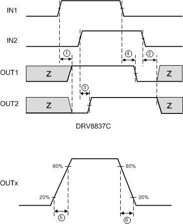 Figure 1. Input and Output Timing for DRV8837C
6.7 Typical Characteristics
Plots generated using characterization data.
| VVM = 5 V | VCC = 3 V |
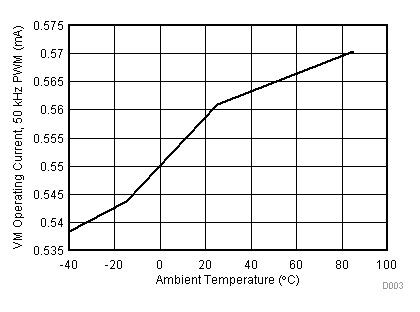
| VVM = 5 V | VCC = 3 V |
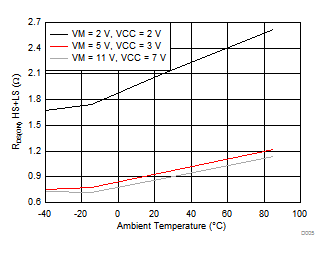 Figure 6. HS + LS RDS(ON) vs Ambient Temperature
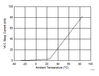
| VVM = 5 V | VCC = 3 V |
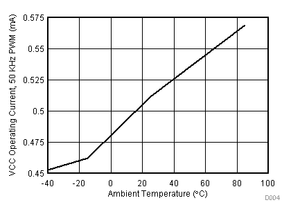
| VVM = 5 V | VCC = 3 V |