ZHCSFB2A July 2016 – July 2016 DRV8837C
PRODUCTION DATA.
10 Layout
10.1 Layout Guidelines
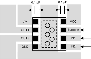
The VM and VCC pins should be bypassed to GND using low-ESR ceramic bypass capacitors with a recommended value of 0.1 µF rated for the VM and VCC supplies. These capacitors should be placed as close to the VM and VCC pins as possible with a thick trace or ground plane connection to the device GND pin. In addition bulk capacitance is required on the VM pin.
10.2 Layout Example
 Figure 13. Simplified Layout Example
10.3 Power Dissipation
Power dissipation in the DRV8837C device is dominated by the power dissipated in the output FET resistance, or RDS(ON). Use Equation 1 to estimate the average power dissipation when running a brushed-DC motor.

where
- PTOT is the total power dissipation
- RDS(ON) is the resistance of the HS plus LS FETs
- IOUT(RMS) is the RMS or DC output current being supplied to the load
The maximum amount of power that can be dissipated in the device is dependent on ambient temperature and heatsinking.
NOTE
The value of RDS(ON) increases with temperature, so as the device heats, the power dissipation increases.
The DRV8837C device has thermal shutdown protection. If the die temperature exceeds approximately 150°C, the device is disabled until the temperature drops to a safe level.
Any tendency of the device to enter thermal shutdown is an indication of either excessive power dissipation, insufficient heatsinking, or too high an ambient temperature.