ZHCS016E January 2011 – July 2015 DRV8833
PRODUCTION DATA.
- 1 特性
- 2 应用
- 3 说明
- 4 修订历史记录
- 5 Pin Configuration and Functions
- 6 Specifications
- 7 Detailed Description
- 8 Application and Implementation
- 9 Power Supply Recommendations
- 10Layout
- 11器件和文档支持
- 12机械、封装和可订购信息
封装选项
请参考 PDF 数据表获取器件具体的封装图。
机械数据 (封装 | 引脚)
- PW|16
- RTY|16
- PWP|16
散热焊盘机械数据 (封装 | 引脚)
- PWP|16
订购信息
10 Layout
10.1 Layout Guidelines
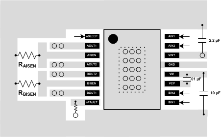
The VM pin should be bypassed to GND using low-ESR ceramic bypass capacitors with a recommended value of 10-μF rated for VM. This capacitor should be placed as close to the VM pin as possible with a thick trace or ground plane connection to the device GND pin.
A low-ESR ceramic capacitor must be placed in between the VM and VCP pins. TI recommends a value of 0.01-μF rated for 16 V. Place this component as close to the pins as possible.
Bypass VINT to ground with a 2.2-μF ceramic capacitor rated 6.3 V. Place this bypass capacitor as close to the pin as possible.
10.1.1 Heatsinking
The PowerPAD package uses an exposed pad to remove heat from the device. For proper operation, this pad must be thermally connected to copper on the PCB to dissipate heat. On a multilayer PCB with a ground plane, this can be accomplished by adding a number of vias to connect the thermal pad to the ground plane. On PCBs without internal planes, copper area can be added on either side of the PCB to dissipate heat. If the copper area is on the opposite side of the PCB from the device, thermal vias are used to transfer the heat between top and bottom layers.
For details about how to design the PCB, refer to TI application report, PowerPAD™ Thermally Enhanced Package (SLMA002) and TI application brief, PowerPAD™ Made Easy (SLMA004), available at www.ti.com.
In general, the more copper area that can be provided, the more power can be dissipated.
NOTE
The PW package option is not thermally enhanced and TI recommends adhering to the power dissipation limits.
10.2 Layout Example
 Figure 10. Recommended Layout Example
10.3 Thermal Considerations
10.3.1 Maximum Output Current
In actual operation, the maximum output current achievable with a motor driver is a function of die temperature. This, in turn, is greatly affected by ambient temperature and PCB design. Basically, the maximum motor current will be the amount of current that results in a power dissipation level that, along with the thermal resistance of the package and PCB, keeps the die at a low enough temperature to stay out of thermal shutdown.
The dissipation ratings given in the data sheet can be used as a guide to calculate the approximate maximum power dissipation that can be expected to be possible without entering thermal shutdown for several different PCB constructions. However, for accurate data, the actual PCB design must be analyzed through measurement or thermal simulation.
10.3.2 Thermal Protection
The DRV8833 has thermal shutdown (TSD) as described above. If the die temperature exceeds approximately 150°C, the device will be disabled until the temperature drops by 45°C.
Any tendency of the device to enter TSD is an indication of either excessive power dissipation, insufficient heatsinking, or too high an ambient temperature.
10.4 Power Dissipation
Power dissipation in the DRV8833 is dominated by the DC power dissipated in the output FET resistance, or RDS(ON). There is additional power dissipated due to PWM switching losses, which are dependent on PWM frequency, rise and fall times, and VM supply voltages. These switching losses are typically on the order of 10% to 30% of the DC power dissipation.
The DC power dissipation of one H-bridge can be roughly estimated by Equation 3.

where
- PTOT is the total power dissipation
- HS - RDS(ON) is the resistance of the high-side FET
- LS - RDS(ON) is the resistance of the low-side FET
- IOUT(RMS) is the RMS output current being applied to the motor
RDS(ON) increases with temperature, so as the device heats, the power dissipation increases. This must be taken into consideration when sizing the heatsink.