ZHCSQ96 July   2021 DRV8770

PRODUCTION DATA  

  1. 特性
  2. 应用
  3. 说明
  4. Revision History
  5. Pin Configuration and Functions
  6. Specifications
    1. 6.1 Absolute Maximum Ratings
    2. 6.2 ESD Ratings Comm
    3. 6.3 Recommended Operating Conditions
    4. 6.4 Thermal Information
    5. 6.5 Electrical Characteristics
    6. 6.6 Typical Characteristics
  7. Detailed Description
    1. 7.1 Overview
    2. 7.2 Functional Block Diagram
    3. 7.3 Feature Description
      1. 7.3.1 Gate Drivers
        1. 7.3.1.1 Gate Drive Timings
          1. 7.3.1.1.1 Propagation Delay
          2. 7.3.1.1.2 Deadtime and Cross-Conduction Prevention
        2. 7.3.1.2 Mode (Inverting and non-inverting INLx)
      2. 7.3.2 Pin Diagrams
      3. 7.3.3 Gate Driver Protective Circuits
        1. 7.3.3.1 VBSTx Undervoltage Lockout (BSTUV)
        2. 7.3.3.2 GVDD Undervoltage Lockout (GVDDUV)
    4. 7.4 Device Functional Modes
  8. Application and Implementation
    1. 8.1 Application Information
    2. 8.2 Typical Application
      1. 8.2.1 Design Requirements
      2. 8.2.2 Detailed Design Procedure
      3. 8.2.3 Application Curves
  9. Power Supply Recommendations
    1. 9.1 Bulk Capacitance Sizing
  10. 10Layout
    1. 10.1 Layout Example
    2. 10.2 Layout Guidelines
  11. 11Device and Documentation Support
    1. 11.1 Receiving Notification of Documentation Updates
    2. 11.2 支持资源
    3. 11.3 Trademarks
    4. 11.4 Electrostatic Discharge Caution
    5. 11.5 术语表
  12. 12Mechanical, Packaging, and Orderable Information

封装选项

请参考 PDF 数据表获取器件具体的封装图。

机械数据 (封装 | 引脚)
  • RGE|24
散热焊盘机械数据 (封装 | 引脚)
订购信息

Pin Diagrams

Figure 7-5 shows the input structure for the logic level pins INHx, INLx. INHx and INLx has passive pull down, so when inputs are floating the output of gate driver will be pulled low. Figure 7-6 shows the input structure for the logic level pin inverted INLx. INLx in inverted mode has passive pull up, so when inputs are floating the output of gate driver will be pulled low.
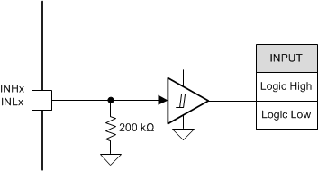
GUID-57DF56EA-90B3-4BAB-974B-6C3B22DEF0EA-low.gifFigure 7-5 INHx and Non-Inverted INLx Logic-Level Input Pin Structure
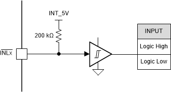
GUID-A6A301B1-A232-47F3-8D40-A0A10E4AF9D7-low.gifFigure 7-6 Inverted INLx Logic-Level Input Pin Structure