ZHCSEB6 October 2015 DRV8704
PRODUCTION DATA.
- 1 特性
- 2 应用
- 3 说明
- 4 修订历史记录
- 5 Pin Configuration and Functions
- 6 Specifications
-
7 Detailed Description
- 7.1 Overview
- 7.2 Functional Block Diagram
- 7.3 Feature Description
- 7.4 Device Functional Modes
- 7.5
Register Maps
- 7.5.1
Control Registers
- 7.5.1.1 CTRL Register (Address = 0x00h)
- 7.5.1.2 TORQUE Register (Address = 0x01h)
- 7.5.1.3 OFF Register (Address = 0x02h)
- 7.5.1.4 BLANK Register (Address = 0x03h)
- 7.5.1.5 DECAY Register (Address = 0x04h)
- 7.5.1.6 Reserved Register Address = 0x05h
- 7.5.1.7 DRIVE Register Address = 0x06h
- 7.5.1.8 STATUS Register (Address = 0x07h)
- 7.5.1
Control Registers
- 8 Application and Implementation
- 9 Power Supply Recommendations
- 10Layout
- 11器件和文档支持
- 12机械、封装和可订购信息
6 Specifications
6.1 Absolute Maximum Ratings
over operating free-air temperature range referenced with respect to GND (unless otherwise noted) (1)| MIN | MAX | UNIT | |
|---|---|---|---|
| Power supply voltage (VM) | –0.6 | 60 | V |
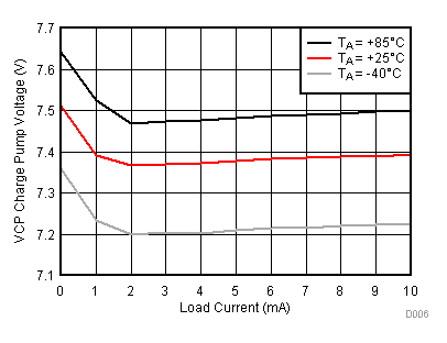
| Charge pump voltage (CP1, CP2, VCP) | –0.6 | VM + 12 | V |
| 5-V regulator voltage (V5) | –0.6 | 5.5 | V |
| Internal regulator voltage (VINT) | –0.6 | 2.0 | V |
| Digital pin voltage (SLEEPn, RESET, AIN1, AIN2, BIN1, BIN2, SCS, SCLK, SDATI, SDATO, FAULTn) | –0.6 | 5.5 | V |
| High-side gate drive pin voltage (A1HS, A2HS, B1HS, B2HS) | –0.6 | VM + 12 | V |
| Low-side gate drive pin voltage (A1LS, A2LS, B1LS, B2LS) | –0.6 | 12 | V |
| Phase node pin voltage (AOUT1, AOUT2, BOUT1, BOUT2) | –0.6 | VM | V |
| ISENSEx pin voltage (AISENP, AISENN, BISENP, BISENN) | –0.7 | +0.7 | V |
| Operating virtual junction temperature, TJ | –40 | 150 | °C |
| Storage temperature, Tstg | –60 | 150 | °C |
(1) Stresses beyond those listed under Absolute Maximum Ratings may cause permanent damage to the device. These are stress ratings only, which do not imply functional operation of the device at these or any other conditions beyond those indicated under Recommended Operating Conditions. Exposure to absolute-maximum-rated conditions for extended periods may affect device reliability.
6.2 ESD Ratings
| VALUE | UNIT | |||
|---|---|---|---|---|
| V(ESD) | Electrostatic discharge | Human-body model (HBM), per ANSI/ESDA/JEDEC JS-001 (1) | ±4000 | V |
| Charged-device model (CDM), per JEDEC specification JESD22-C101 (2) | ±1500 | |||
(1) JEDEC document JEP155 states that 500-V HBM allows safe manufacturing with a standard ESD control process.
(2) JEDEC document JEP157 states that 250-V CDM allows safe manufacturing with a standard ESD control process.
6.3 Recommended Operating Conditions
| MIN | MAX | UNIT | ||
|---|---|---|---|---|
| VM | Motor power supply voltage range | 8 | 52 | V |
| VIN | Digital pin voltage range | 0 | 5.3 | V |
| fPWM | Applied PWM signal (xINx) | 0 | 500 | kHz |
| IV5 | V5 external load current | 0 | 10 | mA |
| TA | Operating ambient temperature range | –40 | 85 | °C |
6.4 Thermal Information
| THERMAL METRIC (1) | DRV8704 | UNIT | |
|---|---|---|---|
| DCP (HTSSOP) | |||
| 38 PINS | |||
| RθJA | Junction-to-ambient thermal resistance | 32.7 | °C/W |
| RθJC(top) | Junction-to-case (top) thermal resistance | 17.2 | °C/W |
| RθJB | Junction-to-board thermal resistance | 14.3 | °C/W |
| ψJT | Junction-to-top characterization parameter | 0.5 | °C/W |
| ψJB | Junction-to-board characterization parameter | 14.1 | °C/W |
| RθJC(bot) | Junction-to-case (bottom) thermal resistance | 0.9 | °C/W |
(1) For more information about traditional and new thermal metrics, see the Semiconductor and IC Package Thermal Metrics application report, SPRA953.
6.5 Electrical Characteristics
TA = 25°C, over recommended operating conditions unless otherwise noted| PARAMETER | TEST CONDITIONS | MIN | TYP | MAX | UNIT | |
|---|---|---|---|---|---|---|
| POWER SUPPLIES (VM) | ||||||
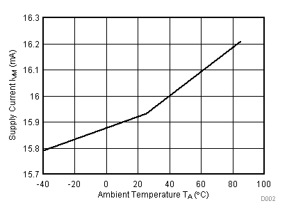
| IVM | VM operating supply current | VM = 24 V | 17 | 22 | mA | |
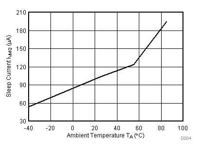
| IVMQ | VM sleep mode supply current | VM = 24 V, SLEEPn low | 65 | 98 | μA | |
| INTERNAL LINEAR REGULATORS (V5, VINT) | ||||||
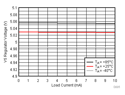
| V5 | V5 output voltage | VM ≥ 12 V, IOUT ≤ 10 mA | 4.8 | 5 | 5.2 | V |
| VINT | VINT voltage | No external load; reference only | 1.7 | 1.8 | 1.9 | V |
| LOGIC-LEVEL INPUTS (SLEEPn, AIN1, AIN2, BIN1, BIN2, RESET, SCLK, SDATI, SCS) | ||||||
| VIL | Input logic low voltage | 0.8 | V | |||
| VIH | Input logic high voltage | 1.5 | V | |||
| VHYS | Input logic hysteresis | 300 | mV | |||
| IIL | Input logic low current | VIN = 0 V | –5 | 5 | μA | |
| IIH | Input logic high current | VIN = 5 V | 24 | 50 | 70 | μA |
| OPEN DRAIN OUTPUTS (nFAULT, SDATO) | ||||||
| VOL | Output logic low voltage | IO = 5 mA | 0.5 | V | ||
| IOH | Output logic high leakage | 10kΩ pullup to 3.3 V | –1 | 1 | μA | |
| GATE DRIVERS | ||||||
| VOUTH | High-side gate drive output voltage | VM = 24 V, IO = 100 μA | VM + 10 | V | ||
| VOUTL | Low-side gate drive output voltage | VM = 24 V, IO = 100 μA | 10 | V | ||
| tDEAD | Output dead time digital delay (dead time is enforced in analog circuits) | DTIME = 00 | 410 | ns | ||
| DTIME = 01 | 460 | |||||
| DTIME = 10 | 670 | |||||
| DTIME = 11 | 880 | |||||
| IOUT,SRC | Peak output sourcing gate drive current | IDRIVEP = 00 | 50 | mA | ||
| IDRIVEP = 01 | 100 | |||||
| IDRIVEP = 10 | 150 | |||||
| IDRIVEP = 11 | 200 | |||||
| IOUT,SNK | Peak output sinking gate drive current | IDRIVEN = 00 | 100 | mA | ||
| IDRIVEN = 01 | 150 | |||||
| IDRIVEN = 10 | 200 | |||||
| IDRIVEN = 11 | 400 | |||||
| tDRIVE,SRC | Peak current drive time for sourcing | TDRIVEP = 00 | 263 | ns | ||
| TDRIVEP = 01 | 525 | |||||
| TDRIVEP = 10 | 1050 | |||||
| TDRIVEP = 11 | 2100 | |||||
| tDRIVE,SNK | Peak current drive time for sinking | TDRIVEN = 00 | 263 | ns | ||
| TDRIVEN = 01 | 525 | |||||
| TDRIVEN = 10 | 1050 | |||||
| TDRIVEN = 11 | 2100 | |||||
| CURRENT REGULATION | ||||||
| tOFF | PWM off time adjustment range | Set by TOFF register | 0.53 | 134 | μs | |
| tBLANK | Current sense blanking time | Set by TBLANK register | 1.05 | 7.0 | μs | |
| AV | Current sense amplifier gain | ISGAIN = 00 | 5 | V/V | ||
| ISGAIN = 01 | 10 | |||||
| ISGAIN = 10 | 20 | |||||
| ISGAIN = 11 | 40 | |||||
| tSET | Settling time (to ±1%) | ISGAIN = 00, ∆VIN = 400 mV | 150 | ns | ||
| ISGAIN = 01, ∆VIN = 200 mV | 300 | |||||
| ISGAIN = 10, ∆VIN = 100 mV | 600 | |||||
| ISGAIN = 11, ∆VIN = 50 mV | 1200 | |||||
| VOFS | Offset voltage | ISGAIN = 00, input shorted | 4 | mV | ||
| VIN | Input differential voltage range | –600 | 600 | mV | ||
| VREF | Internal reference voltage | 2.50 | 2.75 | 3.00 | V | |
| PROTECTION CIRCUITS | ||||||
| VUVLO | Undervoltage lockout | VIN falling; UVLO report | 6.3 | V | ||
| VIN rising; UVLO recovery | 7.1 | 8 | ||||
| VOCP | Overcurrent protection trip level (Voltage drop across external FET) | OCPTH = 00 | 160 | 250 | 320 | mV |
| OCPTH = 01 | 380 | 500 | 580 | |||
| OCPTH = 10 | 620 | 750 | 880 | |||
| OCPTH = 11 | 840 | 1000 | 1200 | |||
| TTSD (1) | Thermal shutdown temperature | Die temperature, TJ | 150 | 160 | 180 | °C |
| THYS (1) | Thermal shutdown hysteresis | Die temperature, TJ | 20 | °C | ||
(1) Not tested in production; limits are based on characterization data
6.6 SPI Timing Requirements
over operating free-air temperature range (unless otherwise noted)| NO. | MIN | MAX | UNIT | ||
|---|---|---|---|---|---|
| 1 | tCYC | Clock cycle time | 250 | ns | |
| 2 | tCLKH | Clock high time | 25 | ns | |
| 3 | tCLCL | Clock low time | 25 | ns | |
| 4 | tSU(SDATI) | Setup time, SDATI to SCLK | 5 | ns | |
| 5 | tH(SDATI) | Hold time, SDATI to SCLK | 1 | ns | |
| 6 | tSU(SCS) | Setup time, SCS to SCLK | 5 | ns | |
| 7 | tH(SCS) | Hold time, SCS to SCLK | 1 | ns | |
| 8 | tL(SCS) | Inactive time, SCS (between writes) | 100 | ns | |
| 9 | tD(SDATO) | Delay time, SCLK to SDATO (during read) | 10 | ns | |
| tSLEEP | Wake time (SLEEPn inactive to high-side gate drive enabled) | 1 | ms | ||
| tRESET | Delay from power-up or RESETn high until serial interface functional | 10 | μs | ||
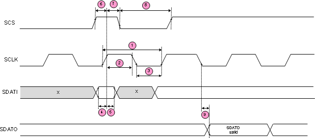 Figure 1. Timing Diagram
6.7 Typical Characteristics
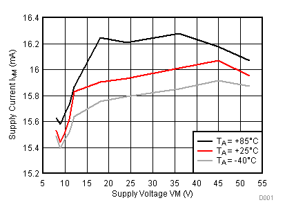
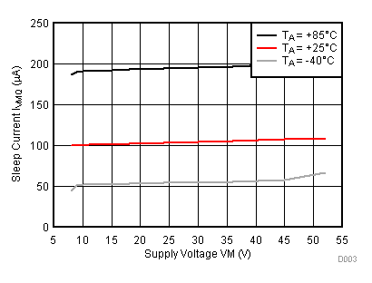
VM = 12 V
VM = 12 V