ZHCSI91B November   2017  – July 2018 DRV8304

UNLESS OTHERWISE NOTED, this document contains PRODUCTION DATA.  

  1. 特性
  2. 应用
  3. 说明
    1.     简化原理图
  4. 修订历史记录
  5. Pin Configuration and Functions
    1.     Pin Functions
  6. Specifications
    1. 6.1 Absolute Maximum Ratings
    2. 6.2 ESD Ratings
    3. 6.3 Recommended Operating Conditions
    4. 6.4 Thermal Information
    5. 6.5 Electrical Characteristics
    6. 6.6 Timing Requirements
    7. 6.7 Typical Characteristics
  7. Detailed Description
    1. 7.1 Overview
    2. 7.2 Functional Block Diagram
    3. 7.3 Feature Description
      1. 7.3.1 3-Phase Smart Gate Drivers
        1. 7.3.1.1 PWM Control Modes
          1. 7.3.1.1.1 6x PWM Mode (PWM_MODE = 00b or MODE Pin Tied to AGND)
          2. 7.3.1.1.2 3x PWM Mode (PWM_MODE = 01b or MODE Pin = 47 kΩ to AGND)
          3. 7.3.1.1.3 1x PWM Mode (PWM_MODE = 10b or MODE Pin = Hi-Z)
          4. 7.3.1.1.4 Independent PWM Mode (PWM_MODE = 11b or MODE Pin Tied to DVDD)
        2. 7.3.1.2 Device Interface Modes
          1. 7.3.1.2.1 Serial Peripheral Interface (SPI)
          2. 7.3.1.2.2 Hardware Interface
        3. 7.3.1.3 Gate Driver Voltage Supplies
        4. 7.3.1.4 Smart Gate-Drive Architecture
          1. 7.3.1.4.1 IDRIVE: MOSFET Slew-Rate Control
          2. 7.3.1.4.2 TDRIVE: MOSFET Gate Drive Control
          3. 7.3.1.4.3 Gate Drive Clamp
          4. 7.3.1.4.4 Propagation Delay
          5. 7.3.1.4.5 MOSFET VDS Monitors
          6. 7.3.1.4.6 VDRAIN Sense Pin
      2. 7.3.2 DVDD Linear Voltage Regulator
      3. 7.3.3 Pin Diagrams
      4. 7.3.4 Low-Side Current-Shunt Amplifiers
        1. 7.3.4.1 Bidirectional Current Sense Operation
        2. 7.3.4.2 Unidirectional Current Sense Operation (SPI only)
        3. 7.3.4.3 Offset Calibration
      5. 7.3.5 Gate-Driver Protection Circuits
        1. 7.3.5.1 VM Supply Undervoltage Lockout (UVLO)
        2. 7.3.5.2 VCP Charge-Pump Undervoltage Lockout (CPUV)
        3. 7.3.5.3 MOSFET VDS Overcurrent Protection (VDS_OCP)
          1. 7.3.5.3.1 VDS Latched Shutdown (OCP_MODE = 00b)
          2. 7.3.5.3.2 VDS Automatic Retry (OCP_MODE = 01b)
          3. 7.3.5.3.3 VDS Report Only (OCP_MODE = 10b)
          4. 7.3.5.3.4 VDS Disabled (OCP_MODE = 11b)
        4. 7.3.5.4 VSENSE Overcurrent Protection (SEN_OCP)
          1. 7.3.5.4.1 VSENSE Latched Shutdown (OCP_MODE = 00b)
          2. 7.3.5.4.2 VSENSE Automatic Retry (OCP_MODE = 01b)
          3. 7.3.5.4.3 VSENSE Report Only (OCP_MODE = 10b)
          4. 7.3.5.4.4 VSENSE Disabled (OCP_MODE = 11b or DIS_SEN = 1b)
        5. 7.3.5.5 Gate Driver Fault (GDF)
        6. 7.3.5.6 Thermal Warning (OTW)
        7. 7.3.5.7 Thermal Shutdown (OTSD)
    4. 7.4 Device Functional Modes
      1. 7.4.1 Gate Driver Functional Modes
        1. 7.4.1.1 Sleep Mode
        2. 7.4.1.2 Operating Mode
        3. 7.4.1.3 Fault Reset (CLR_FLT or ENABLE Reset Pulse)
    5. 7.5 Programming
      1. 7.5.1 SPI Communication
        1. 7.5.1.1 SPI
          1. 7.5.1.1.1 SPI Format
    6. 7.6 Register Maps
      1. Table 1. DRV8304S Register Map
      2. 7.6.1     Status Registers (DRV8304S Only)
        1. 7.6.1.1 Fault Status Register 1 (Address = 0x00) [reset = 0x00]
          1. Table 11. Fault Status Register 1 Field Descriptions
        2. 7.6.1.2 Fault Status Register 2 (Address = 0x01) [reset = 0x00]
          1. Table 12. Fault Status Register 2 Field Descriptions
      3. 7.6.2     Control Registers (DRV8304S Only)
        1. 7.6.2.1 Driver Control Register (Address = 0x02) [reset = 0x00]
          1. Table 14. Driver Control Field Descriptions
        2. 7.6.2.2 Gate Drive HS Register (Address = 0x03) [reset = 0x377]
          1. Table 15. Gate Drive HS Field Descriptions
        3. 7.6.2.3 Gate Drive LS Register (Address = 0x04) [reset = 0x777]
          1. Table 16. Gate Drive LS Register Field Descriptions
        4. 7.6.2.4 OCP Control Register (Address = 0x05) [reset = 0x145]
          1. Table 17. OCP Control Field Descriptions
        5. 7.6.2.5 CSA Control Register (Address = 0x06) [reset = 0x283]
          1. Table 18. CSA Control Field Descriptions
  8. Application and Implementation
    1. 8.1 Application Information
    2. 8.2 Typical Application
      1. 8.2.1 Primary Application
        1. 8.2.1.1 Design Requirements
        2. 8.2.1.2 Detailed Design Procedure
          1. 8.2.1.2.1 External MOSFET Support
            1. 8.2.1.2.1.1 Example
          2. 8.2.1.2.2 IDRIVE Configuration
            1. 8.2.1.2.2.1 Example
          3. 8.2.1.2.3 VDS Overcurrent Monitor Configuration
            1. 8.2.1.2.3.1 Example
          4. 8.2.1.2.4 Sense-Amplifier Bidirectional Configuration
            1. 8.2.1.2.4.1 Example
        3. 8.2.1.3 Application Curves
      2. 8.2.2 Alternative Application
        1. 8.2.2.1 Design Requirements
        2. 8.2.2.2 Detailed Design Procedure
          1. 8.2.2.2.1 Sense-Amplifier Unidirectional Configuration
            1. 8.2.2.2.1.1 Example
  9. Power Supply Recommendations
    1. 9.1 Bulk Capacitance Sizing
  10. 10Layout
    1. 10.1 Layout Guidelines
    2. 10.2 Layout Example
  11. 11器件和文档支持
    1. 11.1 器件支持
      1. 11.1.1 器件命名规则
    2. 11.2 文档支持
      1. 11.2.1 相关文档
    3. 11.3 接收文档更新通知
    4. 11.4 社区资源
    5. 11.5 商标
    6. 11.6 静电放电警告
    7. 11.7 术语表
  12. 12机械、封装和可订购信息

封装选项

请参考 PDF 数据表获取器件具体的封装图。

机械数据 (封装 | 引脚)
  • RHA|40
散热焊盘机械数据 (封装 | 引脚)
订购信息

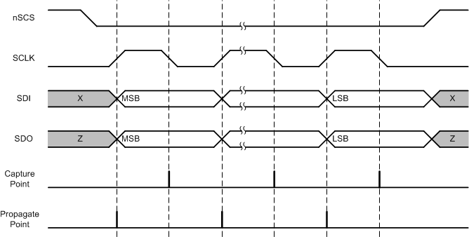
SPI Format

The SDI input data word is 16 bits long and consists of the following format:

  • 1 read or write bit, W (bit B15)
  • 4 address bits, A (bits B14 through B11)
  • 11 data bits, D (bits B11 through B0)

The SDO output data word is 16 bits long and the first 5 bits are don't care bits. The data word is the content of the register being accessed.

For a write command (W0 = 0), the response word on the SDO pin is the data currently in the register being written to.

For a read command (W0 = 1), the response word is the data currently in the register being read.

Table 8. SDI Input Data Word Format

R/W ADDRESS DATA
B15 B14 B13 B12 B11 B10 B9 B8 B7 B6 B5 B4 B3 B2 B1 B0
W0 A3 A2 A1 A0 D10 D9 D8 D7 D6 D5 D4 D3 D2 D1 D0

Table 9. SDO Output Data Word Format

DON'T CARE BITS DATA
B15 B14 B13 B12 B11 B10 B9 B8 B7 B6 B5 B4 B3 B2 B1 B0
X X X X X D10 D9 D8 D7 D6 D5 D4 D3 D2 D1 D0
DRV8304 drv8304-spi-slave-timing-diagram.gifFigure 37. SPI Slave Timing Diagram