ZHCSI91B November   2017  – July 2018 DRV8304

UNLESS OTHERWISE NOTED, this document contains PRODUCTION DATA.  

  1. 特性
  2. 应用
  3. 说明
    1.     简化原理图
  4. 修订历史记录
  5. Pin Configuration and Functions
    1.     Pin Functions
  6. Specifications
    1. 6.1 Absolute Maximum Ratings
    2. 6.2 ESD Ratings
    3. 6.3 Recommended Operating Conditions
    4. 6.4 Thermal Information
    5. 6.5 Electrical Characteristics
    6. 6.6 Timing Requirements
    7. 6.7 Typical Characteristics
  7. Detailed Description
    1. 7.1 Overview
    2. 7.2 Functional Block Diagram
    3. 7.3 Feature Description
      1. 7.3.1 3-Phase Smart Gate Drivers
        1. 7.3.1.1 PWM Control Modes
          1. 7.3.1.1.1 6x PWM Mode (PWM_MODE = 00b or MODE Pin Tied to AGND)
          2. 7.3.1.1.2 3x PWM Mode (PWM_MODE = 01b or MODE Pin = 47 kΩ to AGND)
          3. 7.3.1.1.3 1x PWM Mode (PWM_MODE = 10b or MODE Pin = Hi-Z)
          4. 7.3.1.1.4 Independent PWM Mode (PWM_MODE = 11b or MODE Pin Tied to DVDD)
        2. 7.3.1.2 Device Interface Modes
          1. 7.3.1.2.1 Serial Peripheral Interface (SPI)
          2. 7.3.1.2.2 Hardware Interface
        3. 7.3.1.3 Gate Driver Voltage Supplies
        4. 7.3.1.4 Smart Gate-Drive Architecture
          1. 7.3.1.4.1 IDRIVE: MOSFET Slew-Rate Control
          2. 7.3.1.4.2 TDRIVE: MOSFET Gate Drive Control
          3. 7.3.1.4.3 Gate Drive Clamp
          4. 7.3.1.4.4 Propagation Delay
          5. 7.3.1.4.5 MOSFET VDS Monitors
          6. 7.3.1.4.6 VDRAIN Sense Pin
      2. 7.3.2 DVDD Linear Voltage Regulator
      3. 7.3.3 Pin Diagrams
      4. 7.3.4 Low-Side Current-Shunt Amplifiers
        1. 7.3.4.1 Bidirectional Current Sense Operation
        2. 7.3.4.2 Unidirectional Current Sense Operation (SPI only)
        3. 7.3.4.3 Offset Calibration
      5. 7.3.5 Gate-Driver Protection Circuits
        1. 7.3.5.1 VM Supply Undervoltage Lockout (UVLO)
        2. 7.3.5.2 VCP Charge-Pump Undervoltage Lockout (CPUV)
        3. 7.3.5.3 MOSFET VDS Overcurrent Protection (VDS_OCP)
          1. 7.3.5.3.1 VDS Latched Shutdown (OCP_MODE = 00b)
          2. 7.3.5.3.2 VDS Automatic Retry (OCP_MODE = 01b)
          3. 7.3.5.3.3 VDS Report Only (OCP_MODE = 10b)
          4. 7.3.5.3.4 VDS Disabled (OCP_MODE = 11b)
        4. 7.3.5.4 VSENSE Overcurrent Protection (SEN_OCP)
          1. 7.3.5.4.1 VSENSE Latched Shutdown (OCP_MODE = 00b)
          2. 7.3.5.4.2 VSENSE Automatic Retry (OCP_MODE = 01b)
          3. 7.3.5.4.3 VSENSE Report Only (OCP_MODE = 10b)
          4. 7.3.5.4.4 VSENSE Disabled (OCP_MODE = 11b or DIS_SEN = 1b)
        5. 7.3.5.5 Gate Driver Fault (GDF)
        6. 7.3.5.6 Thermal Warning (OTW)
        7. 7.3.5.7 Thermal Shutdown (OTSD)
    4. 7.4 Device Functional Modes
      1. 7.4.1 Gate Driver Functional Modes
        1. 7.4.1.1 Sleep Mode
        2. 7.4.1.2 Operating Mode
        3. 7.4.1.3 Fault Reset (CLR_FLT or ENABLE Reset Pulse)
    5. 7.5 Programming
      1. 7.5.1 SPI Communication
        1. 7.5.1.1 SPI
          1. 7.5.1.1.1 SPI Format
    6. 7.6 Register Maps
      1. Table 1. DRV8304S Register Map
      2. 7.6.1     Status Registers (DRV8304S Only)
        1. 7.6.1.1 Fault Status Register 1 (Address = 0x00) [reset = 0x00]
          1. Table 11. Fault Status Register 1 Field Descriptions
        2. 7.6.1.2 Fault Status Register 2 (Address = 0x01) [reset = 0x00]
          1. Table 12. Fault Status Register 2 Field Descriptions
      3. 7.6.2     Control Registers (DRV8304S Only)
        1. 7.6.2.1 Driver Control Register (Address = 0x02) [reset = 0x00]
          1. Table 14. Driver Control Field Descriptions
        2. 7.6.2.2 Gate Drive HS Register (Address = 0x03) [reset = 0x377]
          1. Table 15. Gate Drive HS Field Descriptions
        3. 7.6.2.3 Gate Drive LS Register (Address = 0x04) [reset = 0x777]
          1. Table 16. Gate Drive LS Register Field Descriptions
        4. 7.6.2.4 OCP Control Register (Address = 0x05) [reset = 0x145]
          1. Table 17. OCP Control Field Descriptions
        5. 7.6.2.5 CSA Control Register (Address = 0x06) [reset = 0x283]
          1. Table 18. CSA Control Field Descriptions
  8. Application and Implementation
    1. 8.1 Application Information
    2. 8.2 Typical Application
      1. 8.2.1 Primary Application
        1. 8.2.1.1 Design Requirements
        2. 8.2.1.2 Detailed Design Procedure
          1. 8.2.1.2.1 External MOSFET Support
            1. 8.2.1.2.1.1 Example
          2. 8.2.1.2.2 IDRIVE Configuration
            1. 8.2.1.2.2.1 Example
          3. 8.2.1.2.3 VDS Overcurrent Monitor Configuration
            1. 8.2.1.2.3.1 Example
          4. 8.2.1.2.4 Sense-Amplifier Bidirectional Configuration
            1. 8.2.1.2.4.1 Example
        3. 8.2.1.3 Application Curves
      2. 8.2.2 Alternative Application
        1. 8.2.2.1 Design Requirements
        2. 8.2.2.2 Detailed Design Procedure
          1. 8.2.2.2.1 Sense-Amplifier Unidirectional Configuration
            1. 8.2.2.2.1.1 Example
  9. Power Supply Recommendations
    1. 9.1 Bulk Capacitance Sizing
  10. 10Layout
    1. 10.1 Layout Guidelines
    2. 10.2 Layout Example
  11. 11器件和文档支持
    1. 11.1 器件支持
      1. 11.1.1 器件命名规则
    2. 11.2 文档支持
      1. 11.2.1 相关文档
    3. 11.3 接收文档更新通知
    4. 11.4 社区资源
    5. 11.5 商标
    6. 11.6 静电放电警告
    7. 11.7 术语表
  12. 12机械、封装和可订购信息

封装选项

请参考 PDF 数据表获取器件具体的封装图。

机械数据 (封装 | 引脚)
  • RHA|40
散热焊盘机械数据 (封装 | 引脚)
订购信息

Offset Calibration

The DRV8304 device provides an auto calibration feature to minimize the amplifier input offset on power up or during an ENABLE reset pulse to account for temperature and device variation. Auto calibration is performed on both the hardware and SPI device options. The auto calibration begins immediately after the VREF pin crosses the minimum operational VREF voltage and completes in several µs (max 500 µs). During auto calibration, the inputs to the amplifier are disconnected from SPX and SNX pin and shorted internally. After auto calibration the amplifiers are ready for operation.

For the SPI device option, auto calibration can also be performed during run time by setting the AUTOCAL bit. If the AUTOCAL bit is already set once, then the user must reset the bit and again set it to perform the auto-calibration. The user must wait for at least 500 µs before another write to ensure a successful calibration. The user is recommended not to sample CSA outputs during the AUTOCAL operation.

In addition to this, the device also supports an external calibration through the SPI registers (SPI_CAL) in SPI device or through CAL pin in hardware device variant. When the calibration is enabled (CAL pin or SPI_CAL), the inputs to the amplifier are shorted internally, and the amplifier voltage can be observed though SOX pin for doing the external calibration. For the best results, perform offset calibration when the external MOSFETS are not switching to reduce the potential noise impact to the amplifier. DC calibration can be done at any time, even when the half-bridges are operating. Figure 36 shows a diagram of the calibration mode
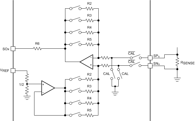
DRV8304 drv8304-amplifier-calibration-mode.gifFigure 36. Amplifier Calibration Mode