ZHCS408C August 2011 – June 2015 DRV201
PRODUCTION DATA.
- 1 特性
- 2 应用
- 3 说明
- 4 修订历史记录
- 5 Pin Configuration and Functions
- 6 Specifications
-
7 Detailed Description
- 7.1 Overview
- 7.2 Functional Block Diagram
- 7.3 Feature Description
- 7.4 Device Functional Modes
- 7.5 Programming
- 7.6
Register Maps
- 7.6.1 Register Address Map
- 7.6.2 Control Register (Control) Address - 0x02h
- 7.6.3 VCM MSB Current Control Register (VCM_Current_MSB) Address - 0x03h
- 7.6.4 VCM LSB Current Control Register (VCM_Current_LSB) Address - 0x04h
- 7.6.5 Status Register (Status) Address - 0x05h
- 7.6.6 Mode Register (Mode) Address - 0x06h
- 7.6.7 VCM Resonance Frequency Register (VCM_FREQ) Address - 0x07h
- 8 Application and Implementation
- 9 Power Supply Recommendations
- 10Layout
- 11器件和文档支持
- 12机械、封装和可订购信息
6 Specifications
6.1 Absolute Maximum Ratings
over operating free-air temperature range (unless otherwise noted) (1)| MIN | MAX | UNIT | ||
|---|---|---|---|---|
| VBAT, ISOURCE, ISINK pin voltage(2) | –0.3 | 5.5 | V | |
| Voltage at SDA, SCL | –0.3 | 3.6 | V | |
| Continuous total power dissipation | Internally limited | |||
| TJ | Operating junction temperature | –40 | 125 | °C |
| TA | Operating ambient temperature | –40 | 85 | °C |
| Tstg | Storage temperature | –55 | 150 | °C |
(1) Stresses beyond those listed under Absolute Maximum Ratings may cause permanent damage to the device. These are stress ratings only, which do not imply functional operation of the device at these or any other conditions beyond those indicated under Recommended Operating Conditions. Exposure to absolute-maximum-rated conditions for extended periods may affect device reliability.
(2) All voltage values are with respect to network ground terminal.
6.2 ESD Ratings
| VALUE | UNIT | ||||
|---|---|---|---|---|---|
| V(ESD) | Electrostatic discharge | Human body model (HBM), per ANSI/ESDA/JEDEC JS-001, all pins(1) | ±4000 | V | |
| Charged device model (CDM), per JEDEC specification JESD22-C101, all pins(2) | ±500 | ||||
(1) JEDEC document JEP155 states that 500-V HBM allows safe manufacturing with a standard ESD control process.
(2) JEDEC document JEP157 states that 250-V CDM allows safe manufacturing with a standard ESD control process.
6.3 Recommended Operating Conditions
over operating free-air temperature range (unless otherwise noted)| MIN | NOM | MAX | UNIT | ||
|---|---|---|---|---|---|
| VBAT - Supply voltage | 2.5 | 3.7 | 4.8 | V | |
| Voltage Range - SDA and SCL | –0.1 | 3.3 | 3.6 | V | |
| TJ - Operating junction temperature | –40 | 125 | °C | ||
6.4 Thermal Information
| THERMAL METRIC(1) | DRV201 | UNIT | ||
|---|---|---|---|---|
| YFM (PICOSTAR) | YMB (DSBGA) | |||
| 6 PINS | 6 PINS | |||
| RθJA | Junction-to-ambient thermal resistance | 130.6 | 116.9 | °C/W |
| RθJC(top) | Junction-to-case (top) thermal resistance | 1.4 | 1.4 | °C/W |
| RθJB | Junction-to-board thermal resistance | 37 | 22.2 | °C/W |
| ψJT | Junction-to-top characterization parameter | 5.2 | 0.1 | °C/W |
| ψJB | Junction-to-board characterization parameter | 37 | 22.2 | °C/W |
(1) For more information about traditional and new thermal metrics, see the Semiconductor and IC Package Thermal Metrics application report, SPRA953.
6.5 Electrical Characteristics
Over recommended free-air temperature range and over recommended input voltage range (typical at an ambient temperature range of 25°C) (unless otherwise noted)| PARAMETER | TEST CONDITIONS | MIN | TYP | MAX | UNIT | ||
|---|---|---|---|---|---|---|---|
| INPUT VOLTAGE | |||||||
| VBAT | Input supply voltage | 2.5 | 3.7 | 4.8 | V | ||
| VUVLO | Undervoltage lockout threshold | VBAT rising | 2.2 | V | |||
| VBAT falling | 2 | ||||||
| VHYS | Undervoltage lockout hysteresis | 50 | 100 | 250 | mV | ||
| INPUT CURRENT | |||||||
| ISHUTDOWN | Input supply current shutdown, includes switch leakage currents | MAX: VBAT = 4.4 V | 0.15 | 1 | µA | ||
| ISTANDBY | Input supply current standby, includes switch leakage currents | MAX: VBAT = 4.4 V | 120 | 200 | µA | ||
| STARTUP, MODE TRANSITIONS, AND SHUTDOWN | |||||||
| t1 | Shutdown to standby | 100 | µs | ||||
| t2 | Standby to active | 100 | µs | ||||
| t3 | Active to standby | 100 | µs | ||||
| t4 | Shutdown time | Active or standby to shutdown | 0.5 | 1 | ms | ||
| VCM DRIVER STAGE | |||||||
| IRES | Resolution | 10 | bits | ||||
| Relative accuracy | –10 | 10 | LSB | ||||
| Differential nonlinearity | –1 | 1 | |||||
| Zero code error | 0 | mA | |||||
| Offset error | At code 32 | 3 | mA | ||||
| Gain error | ±3 | % of FSR | |||||
| Gain error drift | 0.3 | 0.4 | %/°C | ||||
| Offset error drift | 0.3 | 0.5 | %/°C | ||||
| IMAX | Maximum output current | 102.3 | mA | ||||
| ILIMIT | Average VCM current limit | See (1) | 110 | 160 | 240 | mA | |
| IDETCODE | Minimum VCM code for OPEN and SHORT detection | See (2) | 256 | mA | |||
| fSW | Switching frequency | Selectable through CONTROL register | 0.5 | 4 | MHz | ||
| VDRP | Internal dropout | See (3) | 0.4 | V | |||
| LVCM | VCM inductance | 30 | 150 | µH | |||
| RVCM | VCM resistance | 11 | 22 | Ω | |||
| LENS MOVEMENT CONTROL | |||||||
| tset1 | Lens settling time | ±10% error band | 2/fVCM | ms | |||
| tset2 | Lens settling time | ±10% error band | 1/fVCM | ms | |||
| fVCM | VCM resonance frequency | 50 | 150 | Hz | |||
| VCM resonance frequency tolerance | When 1/fVCM compensation is used | –10% | 10% | ||||
| When 2/fVCM compensation is used | –30% | 30% | |||||
| LOGIC I/Os (SDA AND SCL) | |||||||
| IIN | Input leakage current | V = 1.8 V, SCL | –4.25 | 4.25 | µA | ||
| V = 1.8 V, SDA | –1 | 1 | |||||
| RPullUp | I2C pull-up resistors | SDA and SCL pins | 4.7 | kΩ | |||
| VIH | Input high level | See (4) | 1.17 | 3.6 | V | ||
| VIL | Input low level | See (5) | 0 | 0.63 | V | ||
| tTIMEOUT | SCL timeout for shutdown detection | 0.5 | 1 | ms | |||
| RPD | Pull down resistor at SCL line | 500 | kΩ | ||||
| fSCL | I2C clock frequency | 400 | kHz | ||||
| INTERNAL OSCILLATOR | |||||||
| fOSC | Internal oscillator | 20°C ≤ TA ≤ 70°C | –3% | 3% | |||
| Frequency accuracy | -40°C ≤ TA ≤ 85°C | –5% | 5% | ||||
| THERMAL SHUTDOWN | |||||||
| TTRIP | Thermal shutdown trip point | 140 | °C | ||||
(1) During short circuit condition driver current limit comparator will trip and short is detected and driver goes into STANDBY and short flag is set high in the status register.
(2) When testing VCM open or short this is the recommended minimum VCM code (in dec) to be used.
(3) This is the voltage that is needed for the feedback resistor and high side driver. It should be noted that the maximum VCM resistance is limited by this voltage and supply voltage. For example, 3-V supply maximum VCM resistance is: RVCM = (VBAT – VDRP)/IVCM = (3 V - 0.4 V)/102.3 mA = 25.4 Ω.
(4) During shutdown to standby transition VIH low limit is 1.28 V.
(5) During shutdown to standby transition VIL high limit is 0.51 V.
6.6 Data Transmission Timing
VBAT = 3.6 V ±5%, TA = 25ºC, CL = 100 pF (unless otherwise noted)| PARAMETER | TEST CONDITIONS | MIN | TYP | MAX | UNIT | |
|---|---|---|---|---|---|---|
| f(SCL) | Serial clock frequency | 100 | 400 | kHz | ||
| tBUF | Bus Free Time Between Stop and Start Condition | SCL = 100 KHz | 4.7 | µs | ||
| SCL = 400 KHz | 1.3 | |||||
| tSP | Tolerable spike width on bus | SCL = 100 KHz | 50 | ns | ||
| SCL = 400 KHz | ||||||
| tLOW | SCL low time | SCL = 100 KHz | 4.7 | µs | ||
| SCL = 400 KHz | 1.3 | |||||
| tHIGH | SCL high time | SCL = 100 KHz | 4 | µs | ||
| SCL = 400 KHz | 600 | ns | ||||
| tS(DAT) | SDA → SCL setup time | SCL = 100 KHz | 250 | ns | ||
| SCL = 400 KHz | 100 | |||||
| tS(STA) | Start condition setup time | SCL = 100 KHz | 4.7 | µs | ||
| SCL = 400 KHz | 600 | ns | ||||
| tS(STO) | Stop condition setup time | SCL = 100 KHz | 4 | µs | ||
| SCL = 400 KHz | 600 | ns | ||||
| tH(DAT) | SDA → SCL hold time | SCL = 100 KHz | 0 | 3.45 | µs | |
| SCL = 400 KHz | 0 | 0.9 | ||||
| tH(STA) | Start condition hold time | SCL = 100 KHz | 4 | µs | ||
| SCL = 400 KHz | 600 | ns | ||||
| tr(SCL) | Rise time of SCL Signal | SCL = 100 KHz | 1000 | ns | ||
| SCL = 400 KHz | 300 | |||||
| tf(SCL) | Fall time of SCL Signal | SCL = 100 KHz | 300 | ns | ||
| SCL = 400 KHz | 300 | |||||
| tr(SDA) | Rise time of SDA Signal | SCL = 100 KHz | 1000 | ns | ||
| SCL = 400 KHz | 300 | |||||
| tf(SDA) | Rise time of SDA Signal | SCL = 100 KHz | 300 | ns | ||
| SCL = 400 KHz | 300 | |||||
6.7 Typical Characteristics

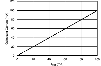
| VBAT = 3.7 V | ||

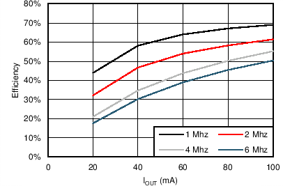
| VBAT = 3.7 V | ||

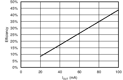
| VBAT = 3.7 V | ||

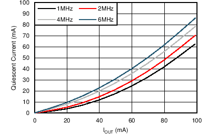
| VBAT = 3.7 V | ||