ZHCS244C January 2012 – August 2015 DLPC300
PRODUCTION DATA.
- 1 特性
- 2 应用
- 3 说明
- 4 修订历史记录
- 5 Pin Configuration and Functions
-
6 Specifications
- 6.1 Absolute Maximum Ratings
- 6.2 ESD Ratings
- 6.3 Recommended Operating Conditions
- 6.4 Thermal Information
- 6.5 I/O Electrical Characteristics
- 6.6 Crystal Port Electrical Characteristics
- 6.7 Power Consumption
- 6.8 I2C Interface Timing Requirements
- 6.9 Parallel Interface Frame Timing Requirements
- 6.10 Parallel Interface General Timing Requirements
- 6.11 Parallel I/F Maximum Supported Horizontal Line Rate
- 6.12 BT.565 I/F General Timing Requirements
- 6.13 Flash Interface Timing Requirements
- 6.14 DMD Interface Timing Requirements
- 6.15 Mobile Dual Data Rate (mDDR) Memory Interface Timing Requirements
- 6.16 JTAG Interface: I/O Boundary Scan Application Switching Characteristics
- 7 Detailed Description
-
8 Application and Implementation
- 8.1 Application Information
- 8.2 Typical Application
- 8.3 System Examples
- 9 Power Supply Recommendations
-
10Layout
- 10.1
Layout Guidelines
- 10.1.1 Printed Circuit Board Design Guidelines
- 10.1.2 Printed Circuit Board Layer Stackup Geometry
- 10.1.3 Signal Layers
- 10.1.4 Routing Constraints
- 10.1.5 Termination Requirements
- 10.1.6 PLL
- 10.1.7 General Handling Guidelines for Unused CMOS-Type Pins
- 10.1.8 Hot-Plug Usage
- 10.1.9 External Clock Input Crystal Oscillator
- 10.2 Layout Example
- 10.3 Thermal Considerations
- 10.1
Layout Guidelines
- 11器件和文档支持
- 12机械、封装和可订购信息
6 Specifications
6.1 Absolute Maximum Ratings
over operating free-air temperature (unless otherwise noted).(1)| MIN | MAX | UNIT | ||
|---|---|---|---|---|
| ELECTRICAL | ||||
| Voltage applied to(2) | VDD10 | –0.5 | 1.32 | V |
| VDD_PLL | –0.5 | 1.32 | V | |
| VCC18 | –0.5 | 2.75 | V | |
| VCC_FLSH | –0.5 | 3.60 | V | |
| VCC_INTF | –0.5 | 3.60 | V | |
| All other input terminals, VO | –0.5 | 3.60 | V | |
| ENVIRONMENTAL | ||||
| TJ | Junction temperature | –30 | 105 | ºC |
| Tstg | Storage temperature | –40 | 125 | ºC |
(1) Stresses beyond those listed under Absolute Maximum Ratings may cause permanent damage to the device. These are stress ratings only, which do not imply functional operation of the device at these or any other conditions beyond those indicated under Recommended Operating Conditions. Exposure to absolute-maximum-rated conditions for extended periods may affect device reliability.
(2) All voltages referenced to VSS (ground).
6.2 ESD Ratings
| VALUE | UNIT | |||
|---|---|---|---|---|
| V(ESD) | Electrostatic discharge | Human body model (HBM), per ANSI/ESDA/JEDEC JS-001, all pins(1) | ±2000 | V |
| Charged device model (CDM), per JEDEC specification JESD22-C101, all pins(2) | ±500 | |||
(1) JEDEC document JEP155 states that 500-V HBM allows safe manufacturing with a standard ESD control process.
(2) JEDEC document JEP157 states that 250-V CDM allows safe manufacturing with a standard ESD control process.
6.3 Recommended Operating Conditions
over operating free-air temperature range (unless otherwise noted). The functional performance of the device specified in this data sheet is achieved when operating the device by the Recommended Operating Conditions. No level of performance is implied when operating the device above or below the recommended operating conditions limits.| MIN | NOM | MAX | UNIT | |||
|---|---|---|---|---|---|---|
| ELECTRICAL | ||||||
| VDD10 | Core logic supply voltage | 0.95 | 1 | 1.05 | V | |
| VDD_PLL | Analog PLL supply voltage | 0.95 | 1 | 1.05 | V | |
| VCC18 | I/O supply voltage (except flash and 24-bit RGB interface signals) | 1.71 | 1.8 | 1.89 | V | |
| VCC_FLSH | Configuration and control I/O supply voltage | 1.8-V LVCMOS | 1.71 | 1.8 | 1.89 | V |
| 2.5-V LVCMOS | 2.375 | 2.5 | 2.625 | |||
| 3.3-V LVCMOS | 3.135 | 3.3 | 3.465 | |||
| VCC_INTF | 24-bit RGB interface supply voltage | 1.8-V LVCMOS | 1.71 | 1.8 | 1.89 | V |
| 2.5-V LVCMOS | 2.375 | 2.5 | 2.625 | |||
| 3.3-V LVCMOS | 3.135 | 3.3 | 3.465 | |||
| VI | Input voltage, all other pins | –0.3 | VCCIO(1) + 0.3 | V | ||
| VO | Output voltage, all other pins | 0 | VCCIO(1) | V | ||
| ENVIRONMENTAL | ||||||
| TJ | Operating junction temperature | –20 | 85 | ºC | ||
(1) VCCIO represents the actual supply voltage applied to the corresponding I/O.
6.4 Thermal Information
| THERMAL METRIC(1) | DLPC300 | UNIT | ||||
|---|---|---|---|---|---|---|
| ZVB (NFBGA) | ||||||
| 176 PINS | ||||||
| RθJC | Junction-to-case thermal resistance | 19.52 | ºC/W | |||
| RθJA | Junction-to-air thermal resistance (with no forced airflow) | 64.96 | ºC/W | |||
(1) For more information about traditional and new thermal metrics, see the Semiconductor and IC Package Thermal Metrics application report, SPRA953.
6.5 I/O Electrical Characteristics
Voltage and current characteristics for each I/O type signal listed in Pin Configuration and Functions. All inputs and outputs are LVCMOS.| PARAMETER | TEST CONDITIONS | MIN | MAX | UNIT | |||
|---|---|---|---|---|---|---|---|
| VIH | High-level input voltage | B64 inputs | VCC = 1.8 V | 1.19 | VCC + 0.3 | V | |
| I1, I2, I3, I4, B14, B18, B34, B38 inputs | 1.2 | VCC + 0.3 | |||||
| I2, I3, B34, B38 inputs | VCC = 2.5 V | 1.7 | VCC + 0.3 | ||||
| I2, I3, B34, B38 inputs | VCC = 3.3 V | 2 | VCC + 0.3 | ||||
| VIL | Low-level input voltage | I1, I2, I3, I4, B14, B18, B34, B38 inputs | VCC = 1.8 V | –0.3 | 0.5 | V | |
| B64 inputs | –0.3 | 0.57 | |||||
| I2, I3, B34, B38 inputs | VCC = 2.5 V | –0.3 | 0.7 | ||||
| I2, I3, B34, B38 inputs | VCC = 3.3 V | –0.3 | 0.8 | ||||
| VOH | High-level output voltage | O14, O24, B14, B34 outputs | VCC = 1.8 V | IOH = –2.58 mA | 1.25 | V | |
| O58 outputs | IOH = = –6.41 mA | 1.25 | |||||
| B18, B38 outputs | IOH = = –5.15 mA | 1.25 | |||||
| O64, O74, B64 outputs | IOH = = –4 mA | 1.53 | |||||
| O24, B34 outputs | VCC = 2.5 V | IOH = = –6.2 mA | 1.7 | ||||
| B38 outputs | IOH = –12.4 mA | 1.7 | |||||
| B38 outputs | IOH = –10.57 mA | 2.4 | |||||
| B38 outputs | VCC = 3.3 V | IOH = –10.57 mA | 1.25 | ||||
| O24, B34 outputs | IOH = –-5.29 mA | 2.4 | |||||
| VOL | Low-level output voltage | O64, O74, B64 outputs | VCC = 1.8 V | IOL = 4 mA | 0.19 | V | |
| O14, O24, B14, B34 outputs | IOL = 2.89 mA | 0.4 | |||||
| B18, B38 outputs | IOL = 5.72 mA | 0.4 | |||||
| O58 outputs | IOL = 5.78 mA | 0.4 | |||||
| O24, B34 outputs | VCC = 2.5 V | IOL = 6.3 mA | 0.7 | ||||
| B38 outputs | IOL = 12.7 mA | 0.7 | |||||
| O24, B34 outputs | VCC = 3.3 V | IOL = 9.38 mA | 0.4 | ||||
| B38 outputs | IOL = 18.68 mA | 0.4 | |||||
6.6 Crystal Port Electrical Characteristics
| PARAMETER | NOM | UNIT |
|---|---|---|
| PLL_REFCLK_I TO GND capacitance | 4.5 | pF |
| PLL_REFCLK_O TO GND capacitance | 4.5 | pF |
6.7 Power Consumption
assumes the transfer of a 12 × 6 checkerboard image in 864 × 480 land scape mode at periodic 30 frames per second over the parallel RGB interface at 25ºC(1)| PARAMETER | TEST CONDITIONS | MIN | NOM | MAX | UNIT |
|---|---|---|---|---|---|
| VCC_INTF | 1.8 V | 0.1 | mW | ||
| VCC_FLSH | 2.5 V | 0 | |||
| VCC18 | 1.8 V | 50.8 | |||
| VDD_PLL | 1 V | 2.8 | |||
| VDD10 | 1 V | 39 |
(1) This table lists the typical current and power consumption of the individual supplies. Note that VCC_FLSH power is 0 because the serial flash is only accessed upon device configuration and not during normal operation.
6.8 I2C Interface Timing Requirements
6.9 Parallel Interface Frame Timing Requirements
| MIN | MAX | UNIT | |||
|---|---|---|---|---|---|
| tp_vsw | Pulse duration – VSYNC high | 50% reference points | 1 | lines | |
| tp_vbp | Vertical back porch – Time from the leading edge of VSYNC to the leading edge HSYNC for the first active line(2) | 50% reference points | 2 | lines | |
| tp_vfp | Vertical front porch – Time from the leading edge of the HSYNC following the last active line in a frame to the leading edge of VSYNC(2) | 50% reference points | 1 | lines | |
| tp_tvb | Total vertical blanking – Time from the leading edge of HSYNC following the last active line of one frame to the leading edge of HSYNC for the first active line in the next frame. (This is equal to the sum of vertical back porch (tp_vbp) + vertical front porch (tp_vfp).) | 50% reference points | 12 | lines | |
| tp_hsw | Pulse duration – HSYNC high | 50% reference points | 4 | 128 | PCLKs |
| tp_hbp | Horizontal back porch – Time from rising edge of HSYNC to rising edge of DATAEN | 50% reference points | 4 | PCLKs | |
| tp_hfp | Horizontal front porch – Time from falling edge of DATAEN to rising edge of HSYNC | 50% reference points | 8 | PCLKs | |
| tp_thh | Total horizontal blanking – Sum of horizontal front and back porches | 50% reference points | See(1) | PCLKs | |
(1) Total horizontal blanking is driven by the maximum line rate for a given source, which is a function of resolution and orientation. See Parallel I/F Maximum Supported Horizontal Line Rate for the maximum line rate for each source/display combination. tp_thb = Roundup[(1000 × ƒclock) / LR] – APPL where ƒclock = Pixel clock rate in MHz, LR = Line rate in kHz, and APPL is the number of active pixels per (horizontal) line. If tp_thb is calculated to be less than tp_hbp + tp_hfp, then the pixel clock rate is too low or the line rate is too high and one or both must be adjusted.
(2) The programmable parameter Vertical Sync Line Delay (I2C: 0x23) must be set such that: 6 – Vertical Front Porch (tp_vfp) (min 0) ≤ Vertical Sync Line Delay ≤ Vertical Back Porch (tp_vbp) – 2 (max 15). The default value for Vertical Sync Line Delay is set to 5; thus, only a Vertical Back Porch less than 7 requires potential action.
6.10 Parallel Interface General Timing Requirements
| MIN | MAX | UNIT | |||
|---|---|---|---|---|---|
| ƒclock | Clock frequency, PCLK | 1 | 33.5 | MHz | |
| tp_clkper | Clock period, PCLK | 50% reference points | 29.85 | 1000 | ns |
| tp_clkjit | Clock jitter, PCLK | Maximum ƒclock | See(1) | ||
| tp_wh | Pulse duration low, PCLK | 50% reference points | 10 | ns | |
| tp_wl | Pulse duration high, PCLK | 50% reference points | 10 | ns | |
| tp_su | Setup time – HSYNC, DATEN, PDATA(23:0) valid before the active edge of PCLK(2) (3) | 50% reference points | 3 | ns | |
| tp_h | Hold time – HSYNC, DATEN, PDATA(23:0) valid after the active edge of PCLK(2) (3) | 50% reference points | 3 | ns | |
| tt | Transition time – all signals | 20% to 80% reference points | 0.2 | 4 | ns |
(1) Clock jitter (in ns) should be calculated using this formula: Jitter = [1 / ƒclock – 28.35 ns]. Setup and hold times must be met during clock jitter.
(2) The active (capture) edge of PCLK for HSYNC, DATEN, and PDATA(23:0) is software programmable, but defaults to the rising edge.
(3) See Figure 3.
6.11 Parallel I/F Maximum Supported Horizontal Line Rate
| DMD | PARALLEL BUS SOURCE RESOLUTION | LANDSCAPE FORMAT(1) | PORTRAIT FORMAT(1) | ||
|---|---|---|---|---|---|
| RESOLUTION (H × V) |
MAX LINE RATE (kHz) |
RESOLUTION (H × V) |
MAX LINE RATE (kHz) |
||
| 0.3 WVGA diamond | NSTC(2) | 720 × 240 | 17 | Not supported | N/A |
| PAL(2) | 720 × 288 | 20 | Not supported | N/A | |
| QVGA | 320 × 240 | 17 | 240 × 320 | 22 | |
| QWVGA | 427 × 240 | 17 | 240 × 427(2) | 27 | |
| 3:2 VGA | 640 × 430 | 30 | 430 × 640 | 45 | |
| 4:3 VGA | 640 × 480 | 34 | 480 × 640 | 45 | |
| WVGA-720 | 720 × 480 | 34 | 480 × 720 | 51 | |
| WVGA-752 | 752 × 480 | 34 | 480 × 752 | 53 | |
| WVGA-800 | 800 × 480 | 34 | 480 × 800 | 56 | |
| WVGA-852 | 852 × 480 | 34 | 480 × 852 | 56 | |
| WVGA-853 | 853 × 480 | 34 | 480 × 853 | 56 | |
| WVGA-854 | 854 × 480 | 34 | 480 × 854 | 56 | |
| WVGA-864 | 864 × 480 | 34 | 480 × 864 | 56 | |
| Optical test | 608 × 684 | 48 | Not supported | N/A | |
(1) See the DLPC300 Software Programmer's Guide (DLPU004) to invoke the appropriate input and output resolutions.
(2) NTSC and PAL are assumed to be interlaced sources.
6.12 BT.565 I/F General Timing Requirements
The DLPC300 controller input interface supports the industry standard BT.656 parallel video interface. See the appropriate ITU-R BT.656 specification for detailed interface timing requirements.(1)| MIN | MAX | UNIT | |||
|---|---|---|---|---|---|
| ƒclock | Clock frequency, PCLK | 1 | 33.5 | MHz | |
| tp_clkper | Clock period, PCLK | 50% reference points | 29.85 | 1000 | ns |
| tp_clkjit | Clock jitter, PCLK | Maximum ƒclock | See(1) | ||
| tp_wh | Pulse duration low, PCLK | 50% reference points | 10 | ns | |
| tp_wl | Pulse duration high, PCLK | 50% reference points | 10 | ns | |
| tp_su | Setup time – HSYNC, DATEN, and PDATA(23:0) valid before the active edge of PCLK | 50% reference points | 3 | ns | |
| tp_h | Hold time – HSYNC, DATEN, and PDATA(23:0) valid after the active edge of PCLK | 50% reference points | 3 | ns | |
| tt | Transition time – all signals | 20% to 80% reference points | 0.2 | 4 | ns |
(1) The BT.656 I/F accepts 8-bit per color, 4:2:2 YCb/Cr data encoded per the industry standard by PDATA(7:0) on the active edge of PCLK (that is, programmable) as shown in Figure 3.
6.13 Flash Interface Timing Requirements
see (2) (3)| MIN | MAX | UNIT | |||
|---|---|---|---|---|---|
| ƒclock | Clock frequency, SPICLK(1) | 33.3266 | 33.34 | MHz | |
| tp_clkper | Clock period, SPICLK | 50% reference points | 29.994 | 30.006 | ns |
| tp_wh | Pulse duration low, SPICLK | 50% reference points | 10 | ns | |
| tp_wl | Pulse duration high, SPICLK | 50% reference points | 10 | ns | |
| tt | Transition time – All signals | 20% to 80% reference points | 0.2 | 4 | ns |
| tp_su | Setup time – SPIDIN valid before SPICLK falling edge | 50% reference points | 10 | ns | |
| tp_h | Hold time – SPIDIN valid after SPICLK falling edge | 50% reference points | 0 | ns | |
| tp_clqv | SPICLK clock low to output valid time – SPIDOUT and SPICS0 | 50% reference points | 1 | ns | |
| tp_clqx | SPICLK clock low output hold time – SPI_DOUT and SPICS0 | 50% reference points | –1 | ns | |
(1) This range includes the 200 ppm of the external oscillator (but no jitter).
(2) Standard SPI protocol is to transmit data on the falling edge of SPICLK and to capture data on the rising edge. The DLPC300 does transmit data on the falling edge, but it also captures data on the falling edge rather than the rising edge. This provides support for SPI devices with long clock-to-Q timing. DLPC300 hold capture timing has been set to facilitate reliable operation with standard external SPI protocol devices.
(3) With the above output timing, DLPC300 provides the external SPI device 14-ns input setup and 14-ns input hold relative to the rising edge of SPICLK.
6.14 DMD Interface Timing Requirements
The DLPC300 controller DMD interface consists of a 76.19-MHz (nominal) DDR output-only interface with LVCMOS signaling.(5)| FROM (INPUT) | TO (OUTPUT) | MIN | MAX | UNIT | |||
|---|---|---|---|---|---|---|---|
| ƒclock | Clock frequency(1) | n/a | DMD_DCLK and DMD_SAC_CLK | 76.198 | 76.206 | MHz | |
| tp_clkper | Clock period | 50% reference points | n/a | DMD_DCLK and DMD_SAC_CLK | 13.123 | 15 | ns |
| tp_wh | Pulse duration low | 50% reference points | n/a | DMD_DCLK and DMD_SAC_CLK | 6.2 | ns | |
| tp_wl | Pulse duration high | 50% reference points | n/a | DMD_DCLK and DMD_SAC_CLK | 6.2 | ns | |
| tt | Transition time | 20% to 80% reference points | n/a | all signals | 0.3 | 2 | ns |
| tp_su | Output setup time (2) (4) | 50% reference points | Both rising and falling edges of DMD_DCLK | DMD_D(14:0), DMD_SCTRL, DMD_LOADB and DMD_TRC | 1.5 | ns | |
| tp_h | Output hold time(2) (4) | 50% reference points | Both rising and falling edges of DMD_DCLK | DMD_D(14:0), DMD_SCTRL, DMD_LOADB, and DMD_TRC | 1.5 | ns | |
| tp_d1_skew | DMD data skew(3) | 50% reference points | Relative to each other | DMD_D(14:0), DMD_SCTRL, DMD_LOADB, and DMD_TRC | 0.2 | ns | |
| tp_clk_skew | Clock skew | 50% reference points | Relative to each other | DMD_DCLK and DMD_SAC_CLK | 0.2 | ns | |
| tp_d2_skew | DAD/SAC data skew | 50% reference points | Relative to DMD_SAC_CLK | DMD_SAC_BUS, DMD_DRC_OE, DMD_DRC_BUS, and DMD_DRC_STRB | 0.2 | ns | |
(1) This range includes the 200 ppm of the external oscillator (but no jitter).
(2) Assumes minimum DMD setup time = 1 ns and minimum DMD hold time = 1 ns
(3) Assumes DMD data routing skew = 0.1 ns max
(4) Output setup/hold numbers already account for controller clock jitter. Only routing skew and DMD setup/hold need be considered in system timing analysis.
(5) Assumes a 30-Ω series termination for all DMD interface signals
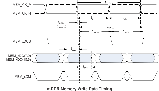
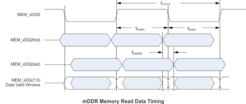
6.15 Mobile Dual Data Rate (mDDR) Memory Interface Timing Requirements
see (2) (3) (4)| MIN | MAX | UNIT | ||
|---|---|---|---|---|
| tCYCLE | Cycle-time reference | 7500 | ps | |
| tCH | CK high pulse duration(5) | 2700 | ps | |
| tCL | CK low pulse duration(5) | 2700 | ps | |
| tDQSH | DQS high pulse duration(5) | 2700 | ps | |
| tDQSL | DQS low pulse duration(5) | 2700 | ps | |
| tWAC | CK to address and control outputs active | –2870 | 2870 | ps |
| tQAC | CK to DQS output active | 200 | ps | |
| tDAC | DQS to DQ and DM output active | –1225 | 1225 | ps |
| tDQSRS | Input (read) DQS and DQ skew(1) | 1000 | ps | |
(1) Note that DQS must be within the tDQSRS read data-skew window, but need not be centered.
(2) This includes the 200 ppm of the external oscillator (but no jitter).
(3) Output setup/hold numbers already account for controller clock jitter. Only routing skew and memory setup/hold must be considered in system timing analysis.
(4) Assumes a 30-Ω series termination on all signal lines
(5) CK and DQS pulse duration specifications for the DLPC300 assume it is interfacing to a 166-MHz mDDR device. Even though these memories are only operated at 133.33 MHz, according to memory vendors, the rated tCK specification (that is, 6 ns) can be applied to determine minimum CK and DQS pulse duration requirements to the memory.
6.16 JTAG Interface: I/O Boundary Scan Application Switching Characteristics
| PARAMETER | TEST CONDITIONS | MIN | MAX | UNIT | |
|---|---|---|---|---|---|
| f(clock) | Clock frequency, JTAGTCK | 10 | MHz | ||
| tc | Cycle time, JTAGTCK | 100 | ns | ||
| tw(L) | Pulse duration low, PCLK | 50% reference points | 40 | ns | |
| tw(H) | Pulse duration high, PCLK | 50% reference points | 40 | ns | |
| tsu | Setup time – JTAGTDI, JTAGTMS; Valid before JTAGTCK↑↓ | 20% to 80% reference points | 8 | ns | |
| th | Hold time – JTAGTDI, JTAGTMS; Valid after JTAGTCK↑↓ | 2 | ns | ||
| tt | Transition time | 5 | ns | ||
| tpd (1) | Output propagation, Clock to Q | From (Input) JTAGTCK↓ to (Output) JTAGTDO | 3 | 12 | ns |
(1) Switching characteristics over Recommended Operating Conditions, CL (minimum timing) = 5 pF, CL (maximum timing) = 85 pF (unless otherwise noted).
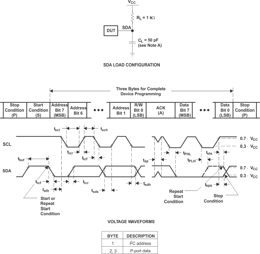
A. ACL includes probe and jig capacitance.
Figure 1. I2C Interface Load Circuit and Voltage Waveforms
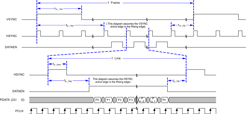 Figure 2. Parallel I/F Frame Timing
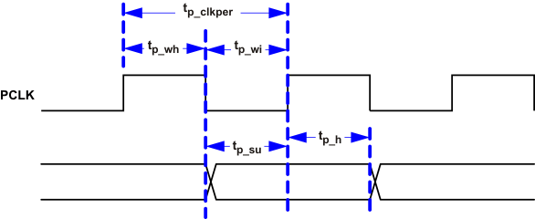 Figure 3. Parallel and BT.656 I/F General Timing
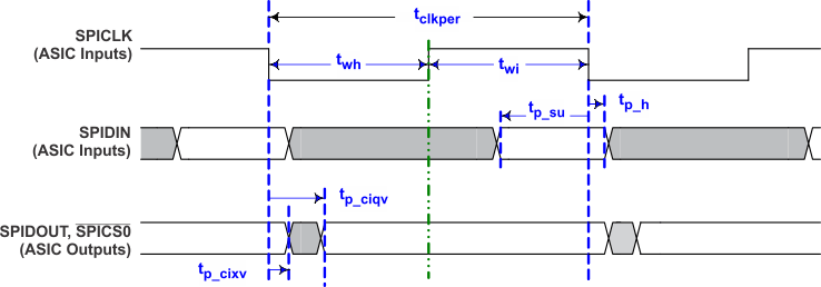 Figure 4. Flash Interface Timing
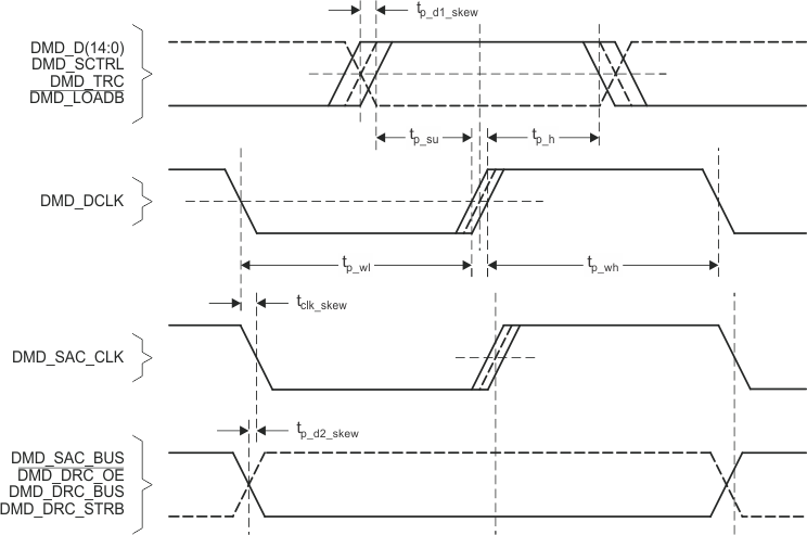 Figure 5. DMD Interface Timing
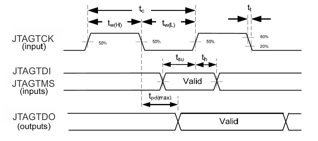 Figure 6. Boundary Scan Timing

