ZHCSI32C october 2018 – july 2023 DLP230GP
PRODUCTION DATA
- 1
- 1 特性
- 2 应用
- 3 说明
- 4 Revision History
- 5 Pin Configuration and Functions
-
6 Specifications
- 6.1 Absolute Maximum Ratings
- 6.2 Storage Conditions
- 6.3 ESD Ratings
- 6.4 Recommended Operating Conditions
- 6.5 Thermal Information
- 6.6 Electrical Characteristics
- 6.7 Timing Requirements
- 6.8 Switching Characteristics
- 6.9 System Mounting Interface Loads
- 6.10 Micromirror Array Physical Characteristics
- 6.11 Micromirror Array Optical Characteristics
- 6.12 Window Characteristics
- 6.13 Chipset Component Usage Specification
- 7 Detailed Description
- 8 Application and Implementation
- 9 Power Supply Recommendations
- 10Layout
- 11Device and Documentation Support
- 12Mechanical, Packaging, and Orderable Information
5 Pin Configuration and Functions
Figure 5-1 FQP Package 54-Pin CLGA Bottom View
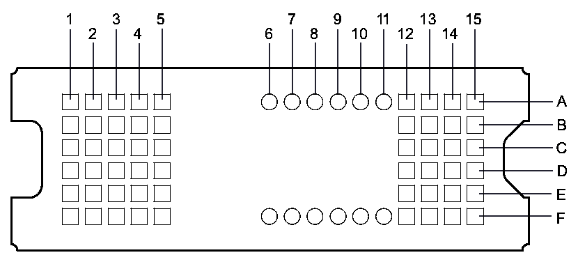
Table 5-1 Connector Pins
| PIN(1) | TYPE | SIGNAL | DATA RATE | DESCRIPTION | PACKAGE NET LENGTH(2) (mm) | |
|---|---|---|---|---|---|---|
| NAME | NO. | |||||
| DATA INPUTS | ||||||
| D_N(0) | A2 | I | SubLVDS | Double | Data, negative | 1.96 |
| D_N(1) | A1 | I | SubLVDS | Double | Data, negative | 1.42 |
| D_N(2) | C1 | I | SubLVDS | Double | Data, negative | 1.35 |
| D_N(3) | B4 | I | SubLVDS | Double | Data, negative | 3.36 |
| D_N(4) | F5 | I | SubLVDS | Double | Data, negative | 4.29 |
| D_N(5) | D4 | I | SubLVDS | Double | Data, negative | 3.20 |
| D_N(6) | E1 | I | SubLVDS | Double | Data, negative | 1.76 |
| D_N(7) | F3 | I | SubLVDS | Double | Data, negative | 2.66 |
| D_P(0) | A3 | I | SubLVDS | Double | Data, positive | 1.97 |
| D_P(1) | B1 | I | SubLVDS | Double | Data, positive | 1.49 |
| D_P(2) | C2 | I | SubLVDS | Double | Data, positive | 1.44 |
| D_P(3) | A4 | I | SubLVDS | Double | Data, positive | 3.45 |
| D_P(4) | E5 | I | SubLVDS | Double | Data, positive | 4.32 |
| D_P(5) | D5 | I | SubLVDS | Double | Data, positive | 3.27 |
| D_P(6) | E2 | I | SubLVDS | Double | Data, positive | 1.85 |
| D_P(7) | F2 | I | SubLVDS | Double | Data, positive | 2.75 |
| DCLK_N | C3 | I | SubLVDS | Double | Clock, negative | 1.94 |
| DCLK_P | D3 | I | SubLVDS | Double | Clock, positive | 2.02 |
| CONTROL INPUTS | ||||||
| LS_WDATA | A12 | I | LPSDR(1) | Single | Write data for low speed interface. | 2.16 |
| LS_CLK | B12 | I | LPSDR | Single | Clock for low-speed interface. | 3.38 |
| DMD_DEN_ARSTZ | B14 | I | LPSDR | Single | Asynchronous reset DMD signal. A low signal places the DMD in reset. A high signal releases the DMD from reset and places it in active mode. | 0.67 |
| DMD_DEN_ARSTZ | F1 | I | LPSDR | Single | 14.90 | |
| LS_RDATA | C13 | O | LPSDR | Single | Read data for low-speed interface. | 2.44 |
| POWER | ||||||
| VBIAS(3) | A15 | Power | Supply voltage for positive bias level at micromirrors. | |||
| VBIAS(3) | A5 | Power | ||||
| VOFFSET(3) | F13 | Power | Supply
voltage for HVCMOS core logic. Supply voltage for stepped high level
at micromirror address electrodes. Supply voltage for offset level at micromirrors. |
|||
| VOFFSET(3) | F4 | Power | ||||
| VRESET | B15 | Power | Supply voltage for negative reset level at micromirrors. | |||
| VRESET | B5 | Power | ||||
| VDD(3) | C15 | Power | Supply voltage for LVCMOS core logic. Supply voltage for LPSDR
inputs. Supply voltage for normal high level at micromirror address electrodes. |
|||
| VDD | C5 | Power | ||||
| VDD | D14 | Power | ||||
| VDD | D15 | Power | ||||
| VDD | E14 | Power | ||||
| VDD | E15 | Power | ||||
| VDD | F14 | Power | ||||
| VDD | F15 | Power | ||||
| VDDI | C14 | Power | Supply voltage for SubLVDS receivers. | |||
| VDDI | C4 | Power | ||||
| VDDI | D13 | Power | ||||
| VDDI | E13 | Power | ||||
| VSS | A13 | Ground | Common return. Ground for all power. |
|||
| VSS | A14 | Ground | ||||
| VSS | B13 | Ground | ||||
| VSS | B2 | Ground | ||||
| VSS | B3 | Ground | ||||
| VSS | C12 | Ground | ||||
| VSS | D1 | Ground | ||||
| VSS | D12 | Ground | ||||
| VSS | D2 | Ground | ||||
| VSS | E12 | Ground | ||||
| VSS | E3 | Ground | ||||
| VSS | E4 | Ground | ||||
| VSS | F12 | Ground | ||||
(1) Low speed interface is LPSDR and adheres to the Electrical
Characteristics and AC/DC Operating Conditions table in JEDEC Standard No. 209B,
Low Power Double Data Rate (LPDDR). See JESD209B.
(2) Net trace lengths inside the package:
Relative dielectric constant for the FQP ceramic package is 9.8.
Propagation speed = 11.8 / sqrt (9.8) = 3.769 in/ns.
Propagation delay = 0.265 ns/inch = 265 ps/in = 10.43 ps/mm.
Relative dielectric constant for the FQP ceramic package is 9.8.
Propagation speed = 11.8 / sqrt (9.8) = 3.769 in/ns.
Propagation delay = 0.265 ns/inch = 265 ps/in = 10.43 ps/mm.
(3) The following power supplies are all required to operate the
DMD: VDD, VDDI, VOFFSET, VBIAS,
VRESET. All VSS connections are also required.
Table 5-2 Test Pads
| NUMBER | SYSTEM BOARD | ||
|---|---|---|---|
| A6 | Do not connect | ||
| A7 | Do not connect | ||
| A8 | Do not connect | ||
| A9 | Do not connect | ||
| A10 | Do not connect | ||
| A11 | Do not connect | ||
| F6 | Do not connect | ||
| F7 | Do not connect | ||
| F8 | Do not connect | ||
| F9 | Do not connect | ||
| F10 | Do not connect | ||
| F11 | Do not connect | ||