SBAS349F August 2005 – June 2016 DAC8812
PRODUCTION DATA.
- 1 Features
- 2 Applications
- 3 Description
- 4 Revision History
- 5 Device Comparison Table
- 6 Pin Configuration and Functions
- 7 Specifications
- 8 Detailed Description
- 9 Application and Implementation
- 10Power Supply Recommendations
- 11Layout
- 12Device and Documentation Support
- 13Mechanical, Packaging, and Orderable Information
11 Layout
11.1 Layout Guidelines
A precision analog component requires careful layout, adequate bypassing, and clean, well-regulated power supplies. The DAC8812 offers single-supply operation, and is often used in close proximity with digital logic, microcontrollers, microprocessors, and digital signal processors. The more digital logic present in the design and the higher the switching speed, the more difficult it is to keep digital noise from appearing at the output. This device has three ground pins: two for analog ground (AGNDA and AGNDB) and one for digital ground (DGND), which are pinned out on opposite sides of the device. Ideally, the analog grounds would be connected directly to an analog ground plane, and similarly the digital ground connected to a digital ground plane. These planes would be separated until they were connected at the power-entry point of the system. The power applied to VDD should be well-regulated and low-noise. Switching power supplies and dc-dc converters often have high-frequency glitches or spikes riding on the output voltage. In addition, digital components can create similar high-frequency spikes as their internal logic switches states. This noise can easily couple into the DAC output voltage through various paths between the power connections and analog output. VDD should be connected to a power-supply plane or trace that is separate from the connection for digital logic until the analog and digital supplies are connected at the power-entry point. In addition, adding both a 100-pF to 1-nF capacitor and a 0.1-μF to 1-μF bypass capacitor is strongly recommended. In some situations, additional bypassing may be required, such as a 100-μF electrolytic capacitor or even a pi filter made up of inductors and capacitors – all designed essentially to provide low-pass filtering for the supply and remove the high-frequency noise.
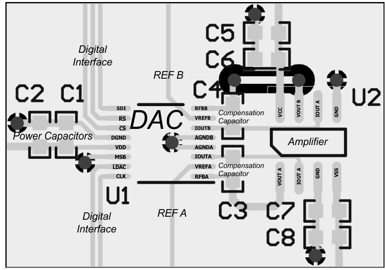
The compensation capacitors shown on the layout in Figure 38 are not required for normal operation of the DAC. However, overshoot of the amplifier output voltage on large code changes is possible. This can be mitigated by using a compensation capacitor between the IOUTx and RFBx nodes, as shown implemented here.
Performance of the DAC8812 can be compromised by grounding and PCB lead trace resistance. The 16-bit DAC8812 with a 10-V full-scale range has an LSB size of 153 µV. The ladder and associated reference and analog ground currents for a given channel can be as high as 2 mA. With this 2-mA current level, a series wiring and connector resistance of only 76 mΩ causes 1 LSB of voltage drop. The preferred PCB layout for the DAC8812 is to have all AGNDx pins connected directly to an analog ground plane at the device. The noninverting input for the transimpedance amplifier of each channel should also either connect directly to the analog ground plane or have an individual sense trace back to the AGNDx pin connection. The feedback resistor trace to the transimpedance amplifier should also be kept short and have low resistance in order to prevent IR drops from contributing to gain error. Therefore, it is important to place the transimpedance amplifier as close to the DAC as possible. This attention to wiring and placement ensures the optimal performance of the DAC8812.
11.2 Layout Example
 Figure 38. DAC8812 Layout Example