SBAS349F August 2005 – June 2016 DAC8812
PRODUCTION DATA.
- 1 Features
- 2 Applications
- 3 Description
- 4 Revision History
- 5 Device Comparison Table
- 6 Pin Configuration and Functions
- 7 Specifications
- 8 Detailed Description
- 9 Application and Implementation
- 10Power Supply Recommendations
- 11Layout
- 12Device and Documentation Support
- 13Mechanical, Packaging, and Orderable Information
9 Application and Implementation
NOTE
Information in the following applications sections is not part of the TI component specification, and TI does not warrant its accuracy or completeness. TI’s customers are responsible for determining suitability of components for their purposes. Customers should validate and test their design implementation to confirm system functionality.
9.1 Application Information
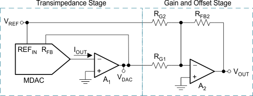
This design features one channel of the DAC8812 followed by a four-quadrant circuit for multiplying DACs. The circuit conditions the current output of an MDAC into a symmetrical bipolar voltage. The design uses an op amp in a transimpedance configuration to convert the MDAC current into a voltage, followed by an additional amplifier in a summing configuration to apply an offset voltage.
9.2 Typical Application
9.2.1 Design Requirements
Using a multiplying DAC requires a transimpedance stage using an amplifier with minimal input offset voltage. The tolerance of the external resistors varies depending on the goals of the application, but for optimal performance with the DAC8812 the tolerance should be 0.1% for all of the external resistors. The summing stage amplifier also requires low input-offset voltage and enough slew rate for the output range desired.
9.2.2 Detailed Design Procedure
The first stage of the design converts the current output of the MDAC (IOUT) to a voltage (VOUT) using an amplifier in a transimpedance configuration. A typical MDAC features an on-chip feedback resistor sized appropriately to match the ratio of the resistor values used in the DAC R-2R ladder. This resistor is available using the input shown in Figure 35 called RFB on the MDAC. The MDAC reference and the output of the transimpedance stage are then connected to the inverting input of the amplifier in the summing stage to produce the output that is defined by Equation 2.

9.2.3 Application Curves
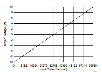
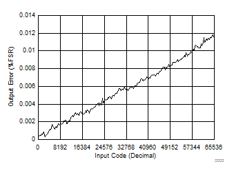
Figure 36 shows the output voltage vs code of this design, and Figure 37 shows the output error vs code. Notice that the error gets worse as the output code increases because the contribution of the DAC gain error increases with code.


