ZHCSEV4A February   2016  – March 2016 DAC8551-Q1

PRODUCTION DATA.  

  1. 特性
  2. 应用
  3. 说明
  4. 修订历史记录
  5. Pin Configuration and Functions
  6. Specifications
    1. 6.1 Absolute Maximum Ratings
    2. 6.2 ESD Ratings
    3. 6.3 Recommended Operating Conditions
    4. 6.4 Thermal Information
    5. 6.5 Electrical Characteristics
    6. 6.6 Timing Requirements
    7. 6.7 Switching Characteristics
    8. 6.8 Typical Characteristics
  7. Detailed Description
    1. 7.1 Overview
    2. 7.2 Functional Block Diagram
    3. 7.3 Feature Description
      1. 7.3.1 DAC Section
        1. 7.3.1.1 Resistor String
        2. 7.3.1.2 Output Amplifier
      2. 7.3.2 Power-On Reset
    4. 7.4 Device Functional Modes
      1. 7.4.1 Power-Down Modes
    5. 7.5 Programming
      1. 7.5.1 SYNC Interrupt
  8. Application and Implementation
    1. 8.1 Application Information
    2. 8.2 Typical Applications
      1. 8.2.1 Loop-Powered 2-Wire 4-mA to 20-mA Transmitter With XTR116
        1. 8.2.1.1 Design Requirements
        2. 8.2.1.2 Detailed Design Procedure
        3. 8.2.1.3 Application Curves
      2. 8.2.2 Bipolar Operation Using the DAC8551-Q1
      3. 8.2.3 Using the REF02 As a Power Supply for the DAC8551-Q1
    3. 8.3 System Examples
      1. 8.3.1 Interface from DAC8551-Q1 to 8051
      2. 8.3.2 Interface from DAC8551-Q1 to Microwire
      3. 8.3.3 Interface from DAC8551-Q1 to 68HC11
  9. Power Supply Recommendations
  10. 10Layout
    1. 10.1 Layout Guidelines
    2. 10.2 Layout Example
  11. 11器件和文档支持
    1. 11.1 文档支持
      1. 11.1.1 相关文档 
    2. 11.2 社区资源
    3. 11.3 商标
    4. 11.4 静电放电警告
    5. 11.5 Glossary
  12. 12机械、封装和可订购信息

封装选项

机械数据 (封装 | 引脚)
散热焊盘机械数据 (封装 | 引脚)
订购信息

10 Layout

10.1 Layout Guidelines

A precision analog component requires careful layout, adequate bypassing, and clean, well-regulated power supplies.

The DAC8551-Q1 offers single-supply operation, and are often used in close proximity with digital logic, microcontrollers, microprocessors, and digital signal processors. The more digital logic present in the design and the higher the switching speed, the more difficult it is to keep digital noise from appearing at the output.

Due to the single ground pin of the DAC8551-Q1, all return currents, including digital and analog return currents for the DAC, must flow through a single point. Ideally, GND would be connected directly to an analog ground plane. This plane would be separate from the ground connection for the digital components until they were connected at the power-entry point of the system.

As with the GND connection, VDD should be connected to a power-supply plane or trace that is separate from the connection for digital logic until they are connected at the power-entry point. In addition, a 1 μF to 10 μF capacitor and 0.1 μF bypass capacitor are strongly recommended. In some situations, additional bypassing may be required, such as a 100 μF electrolytic capacitor or even a Pi filter made up of inductors and capacitors—all designed to essentially low-pass filter the 5 V supply, removing the high-frequency noise.

10.2 Layout Example
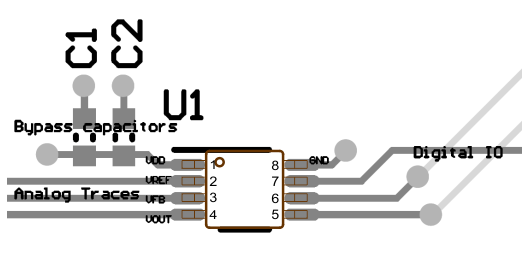
DAC8551-Q1 layout_SLASEB8.gif Figure 40. Layout Diagram