at TA = 25°C,
VDD = VAA = 5 V, VREFIN = 2.5 V, unipolar
ranges: VSS = 0 V and VCC ≥ VMAX + 1.5 V for the
DAC range, bipolar ranges: VSS ≤ VMIN – 1.5 V and
VCC ≥ VMAX + 1.5 V for the DAC range, and DAC outputs
unloaded (unless otherwise noted)
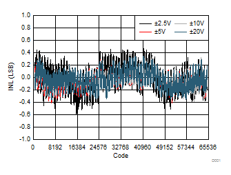 Figure 7-3 Integral Linearity Error vs Digital Input Code (Bipolar Outputs)
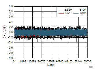 Figure 7-5 Differential Linearity Error vs Digital Input Code (Bipolar Outputs)
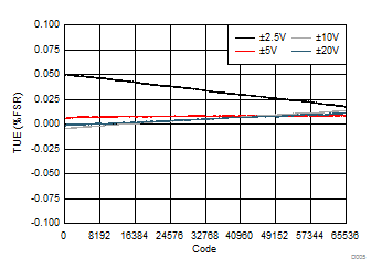 Figure 7-7 Total Unadjusted Error vs Digital Input Code (Bipolar Outputs)
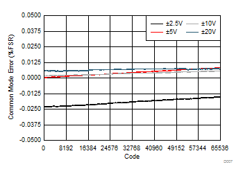 Figure 7-9 Common Mode Error vs Digital Input Code (Differential Bipolar Outputs)
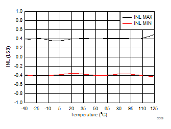 Figure 7-11 Integral Linearity Error vs Temperature
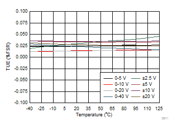 Figure 7-13 Total Unadjusted Error vs Temperature
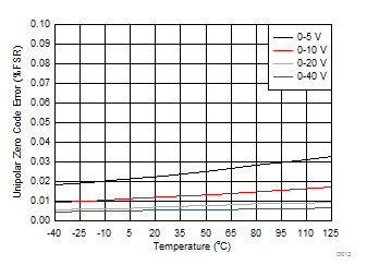 Figure 7-15 Unipolar Zero Code Error vs Temperature
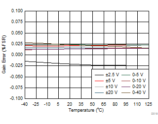 Figure 7-17 Gain Error vs Temperature
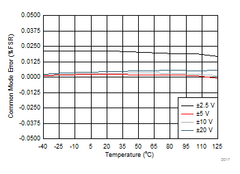 Figure 7-19 Common Mode Error vs
Temperature
(Differential Bipolar
Outputs)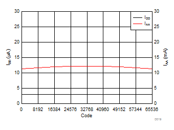 Figure 7-21 Supply Current (IDD, IAA) vs Digital Input Code
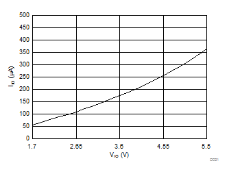 Figure 7-23 Supply Current (IIO) vs Supply Voltage
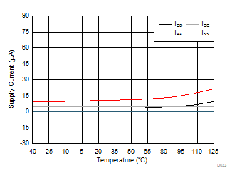 Figure 7-25 Power-Down Current vs Temperature
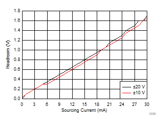 Figure 7-27 VCC Headroom vs Sourcing Current
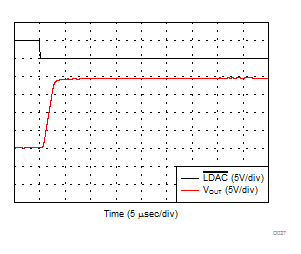 Figure 7-29 Full-Scale Settling Time, Rising Edge
| Power-down to active DAC mode | |
| ±20-V output range | |
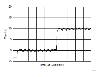
| ±20-V output range | |
| Toggle signal: 1 VPP | |
| DC change: midscale to 3/4 full-scale | |
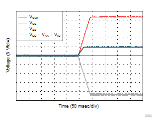 Figure 7-35 Power-Up Response
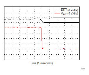
| ±20-V output range | |
| Full-scale code to 0 V | |
| |
|
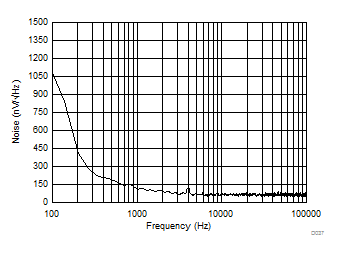
| 0 to 5-V output range | |
| Midscale code | |
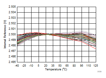 Figure 7-41 Internal Reference Voltage vs Temperature
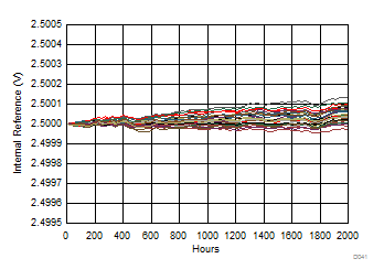 Figure 7-43 Internal Reference Voltage vs Time
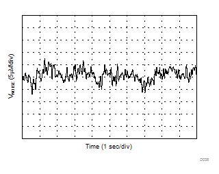
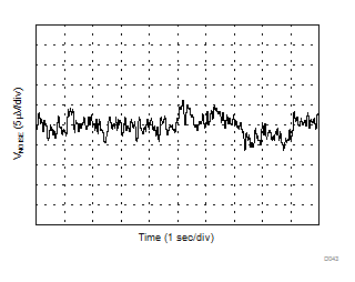 Figure 7-45 Internal Reference Noise
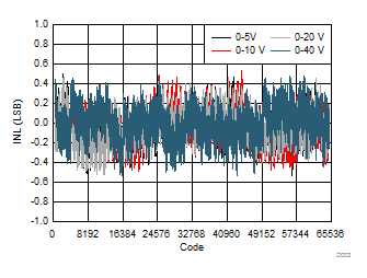 Figure 7-4 Integral Linearity Error vs Digital Input Code (Unipolar Outputs)
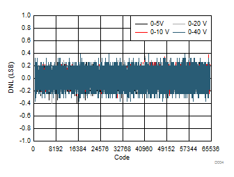 Figure 7-6 Differential Linearity Error vs Digital Input Code (Unipolar Outputs)
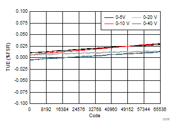 Figure 7-8 Total Unadjusted Error vs Digital Input Code (Unipolar Outputs)
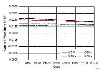 Figure 7-10 Common Mode Error vs Digital Input Code (Differential Unipolar Outputs)
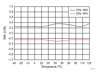 Figure 7-12 Differential Linearity Error vs Temperature
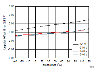 Figure 7-14 Unipolar Offset Error vs Temperature
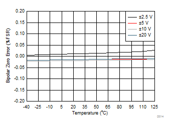 Figure 7-16 Bipolar Zero Error vs Temperature
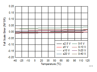 Figure 7-18 Full-Scale Error vs Temperature
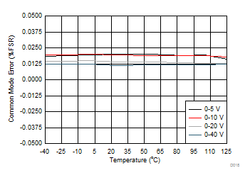 Figure 7-20 Common Mode Error vs
Temperature
(Differential Unipolar
Outputs)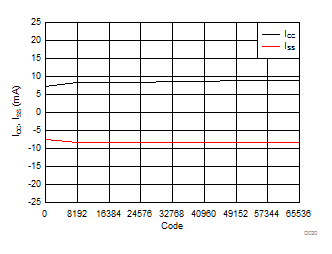 Figure 7-22 Supply Current (ICC, ISS) vs Digital Input Code
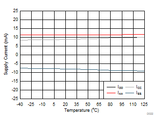 Figure 7-24 Supply Current vs Temperature
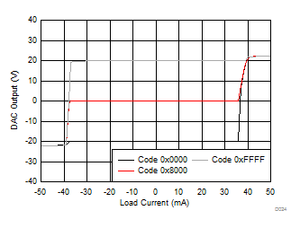 Figure 7-26 Source and Sink Capability
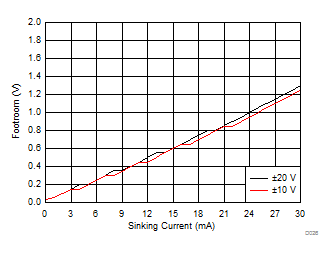 Figure 7-28 VSS Footroom vs Sinking Current
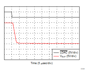 Figure 7-30 Full-Scale Settling Time, Falling Edge
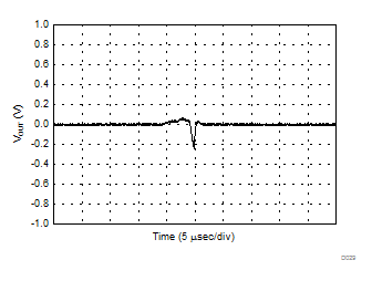
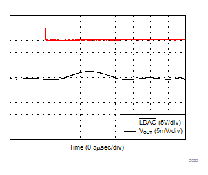 Figure 7-32 Glitch Impulse, 1 LSB Step
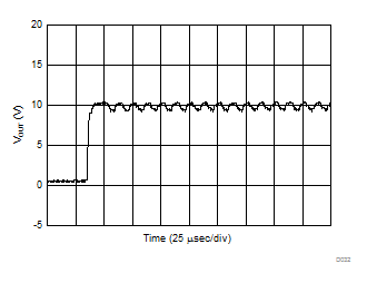
| ±20-V output range | |
| Toggle signal: 1 VPP | |
| DC value: 3/4 full-scale | |
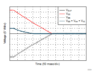 Figure 7-36 Power-Down Response
| ±20-V output range | |
| Toggle signal: 1 VPP | |
| DC value at 20 V | |

| 0 to 5-V output range | |
| Midscale code | |
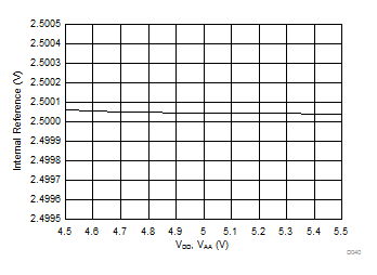
 Figure 7-42 Internal Reference Voltage vs Supply Voltage
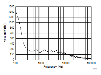
 Figure 7-44 Internal Reference Noise Density vs Frequency
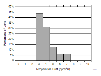
 Figure 7-46 Internal Reference Temperature Drift Histogram


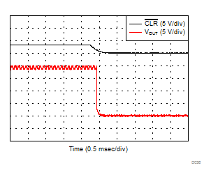
 Figure 7-35 Power-Up Response


 Figure 7-36 Power-Down Response